HTG’s USB 3.0 FMC module: Things you surely want to know
Introduction
I purchased a HiTech Global 3-Port USB 3.0 SuperSpeed FMC Module (also known as USB3 FMC), which is an FPGA Mezzanine Card, primarily based upon TI’s SuperSpeed USB 3.0 Transceiver, TUSB1310A. Even though this board works fine at the end of the day, my experience with it was full with surprises, not all of which were helpful. But first:
Don’t connect the USB/FMC board to the FPGA board before reading through this post. There’s a good chance that the FPGA board will feed the board’s 1.8V power supply with 2.5V, which can potentially damage the USB board permanently. More about that below.
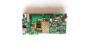
The board has three USB 3.0 connectors, two of which are connected to TUSB1310A transceivers, and one going to a GTX transceiver on the FPGA board. The two photos below show the front and back side of the board. I’ve made the red and green dot markings on the USB Micro-B connectors. The red dot marks the useless connector (explained below), the green one is the one that can be used, and goes to the TUSB1310A. The one not marked is connected directly to the GTX (and is useful, albeit with a few issues).
Click to enlarge photos:


A few minor irritations
These are a few issues that aren’t all that important each by itself, but they mount up. So let’s have them listed.
- The schematics isn’t available until you purchase the board.
- When the package arrived, there was a note telling me to contact support for getting the “product’s documentation for electronic delivery”, as this is an “easy and efficient mechanism for updating the reference designs, user manuals, and other related documents”. What I got was a pdf file with the schematics. That’s it. Meaning, that I had to get the FMC’s pinout from the schematics file. No text-based file (let alone an XDC file for KC705, for example), no user guide, nothing. It’s not just a waste of time to do this manually, but a source for human errors.
- It says (as of writing this) that a USB3 cable is included, but none was. USB 3.0 Micro-B connectors are different from USB 2.0, so if you’re ordering the board, be sure to acquire a cable as well.
- Their rate for shipping & handling was $100. This is just annoyingly high, being roughly twice the commonly required amount. And to be fair about it, there was an alternative method for reducing the shipping costs, which required taking care of the logistics myself. Not really important, but nevertheless annoying.
The FMC VADJ supply voltage
The board’s main power supply is VADJ_FMC, which is connected to the 1.8V power net through a 0 Ohm resistor. VADJ_FMC, as its name implies, is an adjustable voltage, generated by the FPGA board. All Xilinx boards I’m aware of have this voltage set to 2.5V by default. So whoever doesn’t pay attention to this issue, connects several components’ VDD-1.8V to 2.5V. Those of the USB transceivers and clock oscillators, that is.
It would, of course, have been much safer to use the standard 3.3V FMC power supply pins (3P3V, the voltage is standardized), and convert it to 1.8V by means of a DC/DC converter on the board, exactly as the board’s 1.1V supply is generated. It wouldn’t solve the voltage incompatibilities of the I/O connections, but there’s a difference between 2.5V on the power supply and 2.5V on the I/O wires.
Either way, there’s no user manual to warn about this, and no warning note in the schematics. Given the risk to literally blow $800, a piece of paper with a warning written in red, when you open the package, is common practice. There was nothing of this sort.
Even though “VADJ” is an “adjustable voltage”, it doesn’t mean it’s easy to adjust it. As this voltage is generated by a sophisticated power supply controller on all Xilinx’ FPGA boards, it requires reprogramming one of these controllers via PMBUS (which is an I2C-like interface). There are, in principle, two ways for doing this:
- Attaching a USB/PMBUS adapter (available from TI) and programming the power supply with TI’s GUI tool for Windows, Fusion Digital Power. The adapter isn’t expensive ($75 as of writing this), so you probably want to purchase one along with the HTG board.
- Accessing the power supply controller from the FPGA itself. I’ve written a post on this. Doesn’t require purchasing anything, but it may take quite some effort to set it up. Not recommended.
Regardless of the what way chosen, it involves changing one of the many voltages generated on the FPGA board. Depending on how bad you consider blowing the FPGA board to be, you probably want to spend some time getting acquainted with the power supply controllers, which one controls which voltage etc. No matter how you twist and turn it, you’re one little human error away from feeding the FPGA’s core voltage with 12V.
My post on this will probably help, even though it contains a lot of details that aren’t relevant for the recommended GUI tool + adapter route.
To sum this up: VADJ must be set to 1.8V on the FPGA board before the HTG is attached to the FPGA board with the FMC connector. It takes 5 minutes to do this, once you have the USB adapter at hand, the GUI tool installed and running, and the knowledge of exactly which power rail of which controller, at what PMBUS address it answers to.
One TUSB1310A path is (probably) useless
The board has two ports that are connected to TUSB1310A devices, which are in turn connected to the FMC interface. However if the board is attached to any of Xilinx’ primary development kits, KC705, KCU105 or ML605, only one of these ports can be used. I haven’t checked with other FPGA boards, but I’d expect the situation to be the same. Or maybe the second port can be used for USB 2.0 only. I had no interest in the USB 2.0 part, so I didn’t bother to check.
The problem is that not all FMC pins are connected to the FPGA on these FPGA boards: On KC705 and KCU105, neither boards have the FMC connector’s E21-E37 and F21-F37 pins connected to the FPGA, which are used for the PIPE signals on behalf of the USB port connected to J1 (with prefix P2_* on the relevant signal names in the schematics).
As for ML605, it has almost all FMC connections wired, except for four: FMC pins F37, F38, E36 and E37, which are HB20/HB21_P/N. HB20_P/N are assigned to P2_POWER_DOWN0/1 on the HTG board. These pins are disconnected (floating) on ML605. As they are lacking pulldown resistors, neither physically on the board nor by the chip itself, these wires that control the overall power state of the MGT are left floating. So ML605 can’t be used either.
Maybe there is an FPGA board out there that can use both USB ports. Still to find it.
No GTX reference clock
Even though there is a pair of signals intended as a GTX reference clock, GB_CLK_P/N, this clock pair carries no signal. The reason is that the oscillator that produces this 156.25 MHz reference clock, U9, is an TI LMK61E2 with LVPECL output. Unfortunately, the mandatory termination resistors between the LVPECL output and the capacitors are missing. As a result, the LVPECL outputs (BJT transistor’s emitters, current going only one way) just charge the capacitors, with no route to discharge them, so there’s no voltage swing, and hence no clock signal.
The obvious workaround is to use another reference clock, hopefully available on the FPGA board (on KC705 I went for the SGMII ref clock at 125 MHz, pins G7/G8).
By the way, the other identical clock oscillator, U5, generates a clock which is available as four differential clocks on the FMC interface, none of which is classified as an MGT clock on the FMC pinout, so odds are that these aren’t wired to the GTX reference pins on any FPGA board. U5 feeds a clock distributor, U9, which is a Microchip SY89833L without any capacitors in the middle. The latter chip has LVPECL-compatible inputs and LVDS outputs, so there is no problem there. It’s just not helpful for the GTX case. For general-purpose use, they are available as CLKo/1_M2C_P/N.
Design errors with the GTX data path
The board’s third USB port, J3, is intended for a direct connection with the FPGA’s GTX via one of the FMC’s dedicated gigabit pins pairs. There are a few issues to be aware of however:
First, the wire pairs are flipped in polarity in both directions (TX and RX), something that is quite apparent when looking on the FMC connector’s wiring. For example, P3_USB30_SSTX_N is connected to DP0_C2M_P. This is quite harmless, since the GTX has RXPOLARITY and TXPOLARITY ports, which can be asserted to to compensate for this error. And the USB 3.0 spec requires that both sides tolerate an P/N flip. And yet, it’s confusing to see the data stream received by the GTX without knowing about this.
Second, capacitors: There are 100 nF capacitors on the receiving wires of J3 (e.g. P3_USB30_SSRX_N) which shouldn’t be there. The standard for USB 3.0, as well as several other protocols, is that the capacitors are on the transmitting side only. Whoever designed the board knew that, because the capacitors of J1 and J2 are placed correctly (on P{1,2}_USB30_SSTX_{N,P} only).
There is a similar issue with the reference clock that is generated for the gigabit transceiver, GB_CLK_P/N: In this case, there are capacitors on the HTG board as well as the FPGA board. This isn’t really a mistake, because there is no standard on which side should put the capacitors, so both sides played safe. And this doesn’t matter, as this reference clock is dead anyhow, as mentioned above.
Putting two 100 nF capacitors in series yields an equivalent capacitor of 50 nF. For the P3_USB30_SSRX_{N,P} wires, this takes capacitance below the minimum allowed per spec, which is 75 nF. This will hardly have any effect on the gigabit data transmission, but may influence the receiver detection mechanism, which measures the current response to a voltage step. Even though a properly designed USB link partner shouldn’t be this fussy.
And one can always fetch the stereoscope and soldering iron, and replace C10 and C11 with 0 Ohm resistors.
By the way, on KC705, KCU105 (and probably all other Xilinx development kits) they’ve placed 100 nF capacitors on the receiving side only of the SMA GTX connectors (the PCIe fingers are done properly, of course). So trying to connect the USB 3.0 wires to the SMA connectors will not work, unless 100 nF capacitors are added in series with the FPGA’s transmission signals. Go figure.
The XCF constraints for KC705
Since I have it, these are the placement constraints for a KC705, as I figured them out from the schematics of the USB board and Xilinx’ reference XCF for the board. I have tested P1 and P3 as USB 3.0, but that doesn’t guarantee all below is correct. The constraints for P2 aren’t given, because they are useless, as explained above. All single-ended pins are LVCMOS18.
set_property PACKAGE_PIN C27 [get_ports CLK0_M2C_N ] set_property PACKAGE_PIN D27 [get_ports CLK0_M2C_P ] set_property PACKAGE_PIN D18 [get_ports CLK1_M2C_N ] set_property PACKAGE_PIN D17 [get_ports CLK1_M2C_P ]set_property PACKAGE_PIN C8 [get_ports GB_CLK_N ]# No signalset_property PACKAGE_PIN C7 [get_ports GB_CLK_P ]# No signal set_property PACKAGE_PIN C25 [get_ports P1_CLKOUT ] set_property PACKAGE_PIN B24 [get_ports P1_ELAS_BUF_MODE ] set_property PACKAGE_PIN H21 [get_ports P1_GPIO ] set_property PACKAGE_PIN C29 [get_ports P1_PHY_RESET_N ] set_property PACKAGE_PIN B27 [get_ports P1_PHY_STATUS ] set_property PACKAGE_PIN C30 [get_ports P1_PIPE_RX[0] ] set_property PACKAGE_PIN D29 [get_ports P1_PIPE_RX[1] ] set_property PACKAGE_PIN A30 [get_ports P1_PIPE_RX[2] ] set_property PACKAGE_PIN B30 [get_ports P1_PIPE_RX[3] ] set_property PACKAGE_PIN D28 [get_ports P1_PIPE_RX[4] ] set_property PACKAGE_PIN E30 [get_ports P1_PIPE_RX[5] ] set_property PACKAGE_PIN F30 [get_ports P1_PIPE_RX[6] ] set_property PACKAGE_PIN H27 [get_ports P1_PIPE_RX[7] ] set_property PACKAGE_PIN G30 [get_ports P1_PIPE_RX[8] ] set_property PACKAGE_PIN H24 [get_ports P1_PIPE_RX[9] ] set_property PACKAGE_PIN H30 [get_ports P1_PIPE_RX[10] ] set_property PACKAGE_PIN G28 [get_ports P1_PIPE_RX[11] ] set_property PACKAGE_PIN H26 [get_ports P1_PIPE_RX[12] ] set_property PACKAGE_PIN E29 [get_ports P1_PIPE_RX[13] ] set_property PACKAGE_PIN E28 [get_ports P1_PIPE_RX[14] ] set_property PACKAGE_PIN F28 [get_ports P1_PIPE_RX[15] ] set_property PACKAGE_PIN D26 [get_ports P1_PIPE_RX_CLK ] set_property PACKAGE_PIN H25 [get_ports P1_PIPE_RX_K[0] ] set_property PACKAGE_PIN G29 [get_ports P1_PIPE_RX_K[1] ] set_property PACKAGE_PIN G27 [get_ports P1_PIPE_RX_VALID ] set_property PACKAGE_PIN A17 [get_ports P1_PIPE_TX[0] ] set_property PACKAGE_PIN A18 [get_ports P1_PIPE_TX[1] ] set_property PACKAGE_PIN A16 [get_ports P1_PIPE_TX[2] ] set_property PACKAGE_PIN B18 [get_ports P1_PIPE_TX[3] ] set_property PACKAGE_PIN F17 [get_ports P1_PIPE_TX[4] ] set_property PACKAGE_PIN A21 [get_ports P1_PIPE_TX[5] ] set_property PACKAGE_PIN G17 [get_ports P1_PIPE_TX[6] ] set_property PACKAGE_PIN A20 [get_ports P1_PIPE_TX[7] ] set_property PACKAGE_PIN C20 [get_ports P1_PIPE_TX[8] ] set_property PACKAGE_PIN B20 [get_ports P1_PIPE_TX[9] ] set_property PACKAGE_PIN F18 [get_ports P1_PIPE_TX[10] ] set_property PACKAGE_PIN A22 [get_ports P1_PIPE_TX[11] ] set_property PACKAGE_PIN B22 [get_ports P1_PIPE_TX[12] ] set_property PACKAGE_PIN F21 [get_ports P1_PIPE_TX[13] ] set_property PACKAGE_PIN G18 [get_ports P1_PIPE_TX[14] ] set_property PACKAGE_PIN D19 [get_ports P1_PIPE_TX[15] ] set_property PACKAGE_PIN E19 [get_ports P1_PIPE_TX_CLK ] set_property PACKAGE_PIN E21 [get_ports P1_PIPE_TX_K[0] ] set_property PACKAGE_PIN F20 [get_ports P1_PIPE_TX_K[1] ] set_property PACKAGE_PIN B29 [get_ports P1_POWER_DOWN[0] ] set_property PACKAGE_PIN A25 [get_ports P1_POWER_DOWN[1] ] set_property PACKAGE_PIN D21 [get_ports P1_PWRPRESENT ] set_property PACKAGE_PIN D16 [get_ports P1_RATE ] set_property PACKAGE_PIN C21 [get_ports P1_RESET_N ] set_property PACKAGE_PIN F27 [get_ports P1_RX_ELECIDLE ] set_property PACKAGE_PIN A27 [get_ports P1_RX_POLARITY ] set_property PACKAGE_PIN B28 [get_ports P1_RX_STATUS[0] ] set_property PACKAGE_PIN C24 [get_ports P1_RX_STATUS[1] ] set_property PACKAGE_PIN A28 [get_ports P1_RX_STATUS[2] ] set_property PACKAGE_PIN A26 [get_ports P1_RX_TERMINATION ] set_property PACKAGE_PIN G22 [get_ports P1_TX_DEEMPH[0] ] set_property PACKAGE_PIN C16 [get_ports P1_TX_DEEMPH[1] ] set_property PACKAGE_PIN B17 [get_ports P1_TX_DETRX_LPBK ] set_property PACKAGE_PIN C19 [get_ports P1_TX_ELECIDLE ] set_property PACKAGE_PIN F22 [get_ports P1_TX_MARGIN[0] ] set_property PACKAGE_PIN D22 [get_ports P1_TX_MARGIN[1] ] set_property PACKAGE_PIN C22 [get_ports P1_TX_MARGIN[2] ] set_property PACKAGE_PIN B19 [get_ports P1_TX_ONESZEROS ] set_property PACKAGE_PIN C17 [get_ports P1_TX_SWING ] set_property PACKAGE_PIN H14 [get_ports P1_ULPI_CLK ] set_property PACKAGE_PIN A13 [get_ports P1_ULPI_D[0] ] set_property PACKAGE_PIN K16 [get_ports P1_ULPI_D[1] ] set_property PACKAGE_PIN G15 [get_ports P1_ULPI_D[2] ] set_property PACKAGE_PIN B15 [get_ports P1_ULPI_D[3] ] set_property PACKAGE_PIN H16 [get_ports P1_ULPI_D[4] ] set_property PACKAGE_PIN H15 [get_ports P1_ULPI_D[5] ] set_property PACKAGE_PIN L15 [get_ports P1_ULPI_D[6] ] set_property PACKAGE_PIN C15 [get_ports P1_ULPI_D[7] ] set_property PACKAGE_PIN J16 [get_ports P1_ULPI_DIR ] set_property PACKAGE_PIN L16 [get_ports P1_ULPI_NXT ] set_property PACKAGE_PIN K15 [get_ports P1_ULPI_STP ] set_property PACKAGE_PIN E4 [get_ports P3_USB30_SSRX_N ] set_property PACKAGE_PIN E3 [get_ports P3_USB30_SSRX_P ] set_property PACKAGE_PIN D2 [get_ports P3_USB30_SSTX_N ] set_property PACKAGE_PIN D1 [get_ports P3_USB30_SSTX_P ]
Summary
An FMC board for USB 3.0 probably doesn’t sell in large quantities, and it’s quite understandable that its vendor is not interested in spending too much efforts on it. Its design flaws and errors are fairly acceptable once on the table, but given the lack of documentation and supplementary data, the overall picture is not as one would expect from a vendor that has been around for quite a while.
Reader Comments
Eli,
thanks for the wonderful and in-depth review! I wish I would have seen it earlier.
Best Regards,
rudi
Thank you for this good review. Here are a couple things you might find interesting.
The xilinx VC707 board has a fully populated FMC connector which should let you use both PHYs. This board also has a default VADJ voltage of 1.8V which matches the daughter card’s voltage.
Xilinx rocketIO doesn’t support USB3 so the third port that is directly wired to the connector is useless on xilinx boards. I think it may have been added for use on Altera/Intel boards??
Eric
Hi Eli,
Thanks for this post. I recently posted on your Xillybus forum about a USB 3.0 solution, and I’m glad I found this.
So, I have never had a good experience with HiTechGlobal. Many years back I purchased a Virtex-6 evaluation board, but needed it to be pretty top of the line so I got a -3 speed grade chip. The problem was, they used the exact same PCB board for the -3 grade chip that they did for the -1 and -2 grade. Unfortunately, the designers at Hitech didn’t realize that some of the pins are different in between speed grades, so some of my evaluation board pins were routed to literally unconnected FPGA pins. This was especially troublesome when the main clock pin on the board was routed to a normal data pin. Additionally, the PDF they sent along with the board was for the wrong FPGA type, so I had to figure out these myself. The board was $11k, and while they were initially responsive to my asking for help, they stopped responding to my emails after a while.
I have always had bad luck from them in the past, and was considering buying this module, but I don’t think they’ve changed much over the years. They just churn out new models as fast as possible with little quality control.
Hi, Excellent review.. would it possible to share the PDF schematic for this USB3 FMC board?
Regards!
Thanks. Unfortunately, I can’t give it away. Quite obviously, it’s copyrighted material, and in this case it’s clear that its author would dislike me doing so, to say the least.
Thank you, I understand. Do you know if this FMC board is more compatible with an Intel FPGA dev kit like the Cyclone 10 GX dev kit as supposed to a Xilinx as you mentioned?
Regards!
Unfortunately again, I didn’t make this check. I suggest asking HTG — they should provide answers on this matter.
Ok Thank you!
Regards!
Hi Eli,
I recently purchased the Hitech Global FMC USB3 board and I was able to interface the majority of the pins to an Intel FPGA board (Cyclone 10 GX dev kit to be exact). Mainly the PIPE pins and the other various control and status pins were all mapped nicely except for the ULPI pins so USB 2.0 is not supported. Since I have no interest in the USB 2.0 functionality, I didn’t really care too much that these pins did not map and were left floating. As you mentioned, only one of the two TI transceivers can be used. However, I later realized that four of the ULPI data pins are also used for strapping, and if left floating, the chip may behave differently than expected. In my case, pin N6, which is ULPI data bit 7, is left floating and I’m currently having the issue that I cannot receive or transmit data packets. In your experimentation with this FMC USB3 board, did you by any chance come across a similar situation?
By the way, all voltage levels on the Intel board match with this FMC USB3 board so I had mentioned everything maps out nicely except for the ULPI PHY.
Regards,
Luis
Hi,
when I used the fmc3 card into xilinx VC709 board,it is right.but when I put the UART data line access computer,the vc709 board turn off the leds。the vc709′ VADJ is 1.8v。Do you know what’s going on?
Regards。