Controlling the power supplies on a Xilinx KC705 FPGA board with PMBus
You probably don’t want to read all of this
First of all: There is a GUI tool offered by TI to monitor and control its power controller. In hindsight, I have to admit it’s probably the quick & painless way to modify the voltage of a power rail (see this post, not that I’ve tried it). I went for the DYI approach, which turned out by far harder than I imagined. So I suggest reading this, if at all, for a better understanding of what’s going on under the hood. And maybe to understand why you probably don’t want to get into this.
Introduction
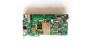
These are the notes I took while making my way to changing the VADJ power supply voltage from its default 2.5V to 1.8V on an KC705 board, for proper operation of an FMC card. One could imagine that it would be easy (remove a jumper?), but the thing is that a rather sophisticated power supply controller (TI UCD9248) is used. In order to make any changes to its output, several parameters need to programmed.
I should mention that similar controllers are used on other Xilinx boards, e.g. ML605, SP605, AC701, VC707, VC709, ZC702 and ZC706, or for short, all or virtually all official Xilinx boards. So the same techniques apply.
To make the necessary programming of the power controller, a rather obscured protocol is used: PMBus. One could, once again, imagine it to be fairly straightforward, as PMBus is based upon SMBus, which is a variant of I2C. The PMBus wires can be accessed from an external connector, or directly from the FPGA.
Unfortunately, the PMBus specification is a multi-nominee for the Oscar of the Worst Written Spec, competing only with Displayport, as far as I can tell. TI’s documentation of the power supply controller family is also somewhat unclear at times.
Xilinx doesn’t help with this issue much either. Even though there are many pointers to AR# 37561 and AR# 56811 in this matter, these offer a solution to return the settings to the factory defaults, or suggest to develop custom code for doing this. Actually, it suggests refraining from making any changes in AR# 37561. KC705′s User Guide, on the other hand, explicitly tells the board’s user to adjust the VADJ voltage, mentions TI’s GUI tool, hints on writing custom code, but doesn’t really say what way to go.
Bottom line: If your FMC card doesn’t work with 2.5V, good luck, and try not burning your FPGA board. Which brings me to:
Warning: Issuing the wrong command to a power supply controller can destroy an FPGA board in a split second. I take no responsibility for any damage, even if something I’ve written is misleading or outright wrong. It’s YOUR full responsibility to double-check any actions against the original documentation.
Quick facts for dropping VADJ to 1.8V on KC705
This is handy no matter what way is chosen:
- The PMBus address of the relevant device is 52
- The voltage rail is 4A, accessed as page 3.
- The original voltage is 2.5V
- All original voltage settings are tuned for 2.5V except for POWER_GOOD_ON = 1.7V and POWER_GOOD_OFF = 1.65 V. So changing just VOUT_COMMAND to 1.8V will probably work, but with an undervoltage fault asserted. Given that this voltage rail can be disabled with a jumper, it’s safe to assume that no other power source depends on it by virtue of sequencing, so this fault is probably harmless. Which is most likely the idea behind this parameter setting.
Resources
This post is by far not a substitute for reading the docs, and taking educated decisions. These are the main documents to get acquainted with:
- The SMBus spec 2.0
- The PMBus spec 1.1, part II
- TI’s UCD92xx Digital PWM System Controller PMBus Command Reference (SLUU337)
- The datasheet for the device in question
There are a few other posts I’ve published along with this one:
- The source code of a logic design for talking with the power controller
- Source code of related utilities
- Output of selected parameters of the power three controllers on KC705
The DYI approach: What needs to be done
In order to make a successful change of a rail voltage, the following is required:
- Setting which power output to control (setting the page, explained below)
- Being aware of, and possibly control the ON/OFF status of the power rail.
- Setting the voltage-related attributes. It’s not just the requested voltage, but also several fault limits etc.
- Writing the new setting into non-volatile memory.
PMBus vs. SMBus vs. I2C
The PMBus specification defines four pins, unlike the two pins (clock and data) most of us are used to from I2C and SMBus. UCD92xx devices present all four PMBus pins. One of the “new” pins is ALERT, which is defined in the SMBus spec as SMBALERT. This pin is used as an interrupt from the device to the master, in particular for reporting faults. For the purpose of changing voltages, this pin can be ignored.
The second pin is introduced in the PMBus spec: CONTROL. This pin is optionally used to turn all power rails on or off, possibly is a sequenced manner. It’s usually tied high on Xilinx boards, and doesn’t help much: If we want to control a specific power rail, it’s wiser to do so by sending commands, rather than turning the entire controller on and off with this pin. Assuming that the controller is configured to react to this pin, that is. More on this later.
For most purposes, PMBus is SMBus, and SMbus is I2C, so an I2C-compliant bus master will most likely do the trick. One needs to bear in mind that the byte following the bus address isn’t a register address, but a command. The difference is that when several data bytes are transmitted, there is no register address incrementation. For example, for setting the overvoltage fault limit, the bus address is followed by an 0x40 (VOUT_OV_FAULT_LIMIT command) which is then followed by a word — that is, two bytes. Had it been an I2C bus, the second byte would have gone to the register at 0x41. But there is no auto-incremented address with PMBUS. The command at 0x41, VOUT_OV_FAULT_RESPONSE remains intact.
Except for the lack of address auto-increment, PMBus is used like an I2C bus, where the command takes the place of a single-byte I2C address. In particular, reading takes place with a write operation without data, followed by an start-stop condition, and then a read cycle.
So the term “command” can be treated as an I2C register for most purposes.
But well, there’s another important exception, which is the set of no-data commands. It’s those having Transaction Type “Send Byte” in Table-1 of SLUU337. These transactions end immediately after the command, so from an I2C-register point of view, they did nothing. But on a PMBus, such a sequence can do serious things, for example, the RESTORE_DEFAULT_ALL command, which can have unpleasant consequences.
As for attempting to read from this “command address”, it could, in theory, result in the same effect as writing to it, because a read transaction’s first part is a command without data. There is a difference, however: There’s a restart after the first part, and not a STOP condition. My experiment with UCD9240 shows that the device noted this difference, and responded with not executing a CLEAR_FAULTS command (for other errors than this communication fault). As for the part after the restart condition, it acknowledged its own address (as it’s forced to per spec) but forced the PMBus clock signal low immediately after that, thus freezing the bus transaction, causing a recovery by means of an SMBus timeout. So this specific device played it well, but I wouldn’t rely on this.
SMBus allows for an extra PEC byte at the end of each transaction, which is a CRC. This is optional with PMBus. The UCD92xx devices support PEC, but work without it. I’ve personally verified that the device responds correctly with and without the PEC byte inserted or retrieved from the device. I’ve also verified that a write cycle with a faulty PEC is ignored by the device, which is the reason I use this mechanism myself: Given the price of a flipped bit (literally), I really want to know if the bus is anything but bulletproof.
UCD92xx’s PMBus robustness
It seems like the UCD92xx’s PMBus implementation doesn’t fall on its feet as well as other I2C / SMBus devices I’ve encountered: In particular, a previous version of my own hacky implementation of an I2C/SMBus master didn’t finish read transaction correctly, but issued a STOP condition after the last read byte, instead of NACKing and then issue a STOP, as it should per spec (this is fixed in the published code). A lot of other I2C devices I’ve worked with (many of which from TI) ignore this mishap, and followed the (unwritten?) rule that a STOP condition means forgive & forget, and the following START means a fresh start. The UCD9240 device, on the other hand, returned all 0xff on the read cycle that followed the offending one. And then returned correct data on the read cycle after that, even though it had exactly the same fault.
This anecdotal incident may imply that UCD92xx devices may not react well to bus masters that have protocol flaws that other slaves ignore silently. It doesn’t make UCD92xx devices safer, just a bit picky.
I also ended up with a bus clock frequency of 8 kHz only, even though the datasheet ensures up to 400 kHz. The reason was that when I tried two consecutive read commands with a 32 kHz clock, the second consistently returned an all-0xff answer, most likely because the device’s firmware didn’t keep up with the read requests.
Page vs. power rail
The UCD92xx devices on Xilinx boards are used to control several voltage sources. Each voltage source can be driven by one or more PWM-controlled power front ends (on Xilinx boards, there’s always one front-end for each voltage).
The PMBus specification facilitates the control of multiple power rails by a single controller with pages. So to control the voltage of a specific voltage source, the page is selected first by a write transaction with a PAGE (0x00) command. After this command, a certain set of commands relate to this page — effectively all commands that are bound to a voltage rail: Desired voltage, fault limits of voltage and current, the sensed voltage and current etc.
The relation between the page and the physical rail it controls is programmable. By no means should it be assumed that PAGE 0 relates to the lowest index of the physically controlled power lines or anything like that. In a given system, this mapping is obtained by issuing a PHASE_INFO (0xd2) read command, and analyzing the response. It’s of course crucial to make this connection correctly before changing the setting of any PAGE, or the wrong power rail is affected. Refer to TI’s reference on UCD92xx commands (SLUU337) section 10.1 for more on this, and the sample utils demonstrate how this relation is made. It can also be seen in Linux kernel’s driver (drivers/hwmon/pmbus/ucd9200.c), which issues a PHASE_INFO read command in its probe function, and deduces the number of pages according to the response. According to TI’s doc on UCD92xx commands (SLUU337) section 10.1.1, no gaps are allowed in the page allocation, so this way of telling the maximal allowed page number is correct.
A UCD92xx device refuses to switch to a PAGE command if the related page is unused, as reflected by the response to a PHASE_INFO read command. In other words, the device refuses to switch to a page for which no power rail phases are attached, according to PHASE_INFO. Such refusal takes the form of a PMBus NAK on the byte containing the requested page (the one followed by the command byte) and the current page remaining unchanged. This behavior seems not to be documented by TI or have any other written reference.
There is also a similar division of a page into phases, but this is irrelevant, as each page is mapped into a single phase (i.e. uses a single PWM output) on Xilinx’ boards. So this entire issue can be overlooked. Except for knowing which phase (PWM output) is mapped to which page, of course.
The on/off status
Mainly two commands control whether the power rail is on or off, and which voltage is supplies: OPERATION (0x01) and ON_OFF_CONFIG (0x02). UCD92xx devices follow the PMBus standard in this matter.
Except for these two commands, sequencing is controlled by the manufacturer-specific commands GPIO_SEQ_CONFIG (0xf3) and SEQ_TIMEOUT (0xd0). The former is a 29-bytes long block of configuration bitmaps, which is a bit of a story in itself. For those curious to understand how the J65 jumper on KC705 enables the VADJ power rail, this is where to look. Also if the powerup sequencing is of interest.
Otherwise, and in particular for the purpose of a single voltage modification, these two sequencing-related commands are not worth further attention.
As for OPERATION and ON_OFF_CONFIG, their somewhat tangled definitions can found in the PMBus spec. Apparently, the power rail can be controlled with these commands, but I never got down to the details of this, mainly because I didn’t want to make any unnecessary experiments with the FPGA board.
I should mention that the typical setting on all power rails is ON_OFF_CONFIG = 0x02 or 0x00, which means ignoring the CONTROL input pin for the rail, and OPERATION = 0x40, which means that the power rail is turned off (with sequencing). So why is the power rail on? The only possibility left is that sequencing brought it up. The docs are somewhat lacking.
For direct control of the power rail I would try (following the positive experience reported in the green frame on this post) setting ON_OFF_CONFIG to 0x1a, and then writing 0x00 to OPERATION for turning the power rail off, and 0x80 for turning it on. Note that the OPERATION state is never stored into non-volatile memory on an UCD92xx.
Storing to non-volatile memory
All commands change the values in the power controller’s RAM (“Operating Memory”). The next time it’s powered on, defaults are loaded from an on-chip flash.
To store the current setting as power-on defaults, an STORE_DEFAULT_ALL (0x11) command is issued. It’s one of those no-data commands.
Numeric representation
Several commands represent physical parameters, such as voltage, current and temperature. The numerical format of these values is unfortunately a bit of a disaster. There are three formats used by the UCD92xx family, named below as they appear in Table 1 in SLUU337:
- LINEAR16: The primary format for voltages. It’s a 16-bit, unsigned fixed-point fractional 4.12 representation of the voltage. This spans between 0V and almost 16 V, with a 0.2441 mV resolution. The voltage is obtained from the 16-bit word with
unsigned short word;
double voltage = word / 4096.0;
- LINEAR16, signed: Used by the VOUT_CAL_OFFSET command. Same as LINEAR16, only “word” is of signed short type.
- LINEAR11: The format used for all other non-integer parameters. This is an unsigned 16-bit floating-point word with an 11-bit mantissa and a 5-bit exponent. The parameter is obtained with
unsigned short word;
double x = word & 0x7ff;
int exponent = (word >> 11) & 0xf;

if (word & 0x8000)
  x /= 1 << (16 - exponent);
else
  x *= 1 << exponent;
Note that other PMBus-based controllers probably use other formats (the PMBus spec allows a variety).
The sample C utils include the conversions of the numeric formats, of course.
At last: How to change the voltage
This is the list of voltage commands to make in order to reduce the output voltage, without turning it off. The point is to avoid any faulty conditions on the way, so the transition is smooth. This is done by lowering the limits for undervoltage first, then dropping the actual voltage to the target voltage. After that, lower the limits for overvoltage.
But before any of these, change two parameters that are probably unused generally, and surely not in effect during the operation: VOUT_MARGIN_HIGH and VOUT_MARGIN_LOW. These are relevant only when one of the “margin” modes are selected with the OPERATION command, which is probably never. The idea is to start with commands that don’t make much difference anyhow, just in case something goes wrong.
Those choosing to turn off the power rail before making the changes may update the parameters in any order.
So these are the commands, in order of execution. The commonly used diversion from the nominal voltage is given in parentheses.
- VOUT_MAX: This parameter is intended to protect the circuitry from a voltage too high. It stands at 3.6328V on almost all rails of KC705, so just leave it as is (On SP605 it’s on 10.6890V, which is rather pointless).
- VOUT_MARGIN_HIGH (+5%): The voltage to output when OPERATION is set to output Margin High. Probably makes no difference.
- VOUT_MARGIN_LOW (-5%): Same as VOUT_MARGIN_HIGH, only with Margin Low output.
- POWER_GOOD_ON (-5%): The voltage threshold which turns the “power good” state on. Note that “power good” isn’t just an output pin, but may also influence the powerup sequencing machine.
- POWER_GOOD_OFF (-8%): The voltage at which “power good” is deasserted. Being slightly lower than POWER_GOOD_ON, there’s a Schmitt-trigger effect.
- VOUT_UV_WARN_LIMIT (-10%): The voltage under which a warning condition is issued (except during ramp-up and when the rail is turned off).
- VOUT_UV_FAULT_LIMIT (-12% to -15%): The voltage under which a fault condition is issued (except during ramp-up and when the rail is turned off). This may, among others, lead to the rail’s shutdown, as defined in VOUT_UV_FAULT_RESPONSE. However sequencing interdependencies may take down other rails as well following such fault.
- VOUT_COMMAND: The desired output voltage. The point of the entire saga.
- VOUT_OV_WARN_LIMIT (+12% to +15%): The voltage over which a warning condition is issued.
- VOUT_OV_FAULT_LIMIT (+10%): The voltage over which a fault condition is issued. VOUT_OV_FAULT_RESPONSE controls the behavior on such fault, and sequencing interdependencies have the same effect as with VOUT_UV_FAULT_LIMIT.
In order to change the target voltage upwards, reverse the order, except for keeping VOUT_MARGIN_HIGH and VOUT_MARGIN_LOW at the beginning.
Random notes
- Current readings may be incorrect (usually zero) if no current sensors are connected to the rail’s CS input(s). This is the case on some power rails of SP605, for example. The power source functions properly nevertheless.
- Appendix I of Part II of the PMBus spec outlines not only the commands, but the SMBus transaction types for each (most are trivial however).
Good luck, and may the power be with you.
Reader Comments
Here are a couple tips/corrections that might help…
You got 0xFF results after an inadvertent STOP condition because no PMBus transaction may begin with a the “read bit” in the device address. If you don’t do the repeated start, you really are starting fresh; there’s no memory of the previous command code.
Second – the LINEAR11 format is signed. Both the 5-bit exponent and the 11-bit mantissa are two’s complement numbers.