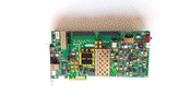
Test point placement constraints for KC705
The said board, which is Xilinx’ official development kit for Kintex-7, has an LCD which can be taken off. Its pins can then be used as plain testpoints for logic. These are the placement constraint for this use (Vivado XDC style):
set_property PACKAGE_PIN Y10 [get_ports tp[0]]; # LCD_DB7, pin 1
set_property PACKAGE_PIN AA11 [get_ports tp[1]]; # LCD_DB6, pin 2
set_property PACKAGE_PIN AA10 [get_ports tp[2]]; # LCD_DB5, pin 3
set_property PACKAGE_PIN AA13 [get_ports tp[3]]; # LCD_DB4, pin 4
set_property PACKAGE_PIN AB10 [get_ports tp[4]]; # LCD_E, pin 9
set_property PACKAGE_PIN AB13 [get_ports tp[5]]; # LCD_RW, pin 10
set_property PACKAGE_PIN Y11 [get_ports tp[6]]; # LCD_RS, pin 11

set_property IOSTANDARD LVCMOS15 [get_ports tp[*]]

set_false_path -to [get_ports -filter {NAME=~tp[*]}]
The actual voltage on these pins is 3.3V — there’s a voltage shifter inbetween, which is why these pins can’t be used as inputs.