Intel FPGA’s Stratix 10: My impressions and notes
Posted Under: FPGA,Intel FPGA (Altera),PCI express
Introduction
These are a few random things I wrote down as I worked with the Stratix 10 Development Kit, with focus on its PCIe interface. Quite obviously, it’s mostly about things I found noteworthy about this specific FPGA and its board, compared with previous hardware I’ve encountered.
Generally speaking, Stratix 10 is not for the faint-hearted: It has quite a few special issues that require attention when designing with it (some detailed below), and it’s clearly designed with the assumption that if you’re working with this king-sized beast, you’re most likely part of some high-end project, being far from a novice in the FPGA field.
Some National Geographic
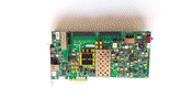
Even though I discuss the development kit further below, I’ll start with a couple of images of the board’s front and back. This 200W piece of logic has a liquid cooler and an exceptionally noisy fan — none of which are shown in Intel’s official images I’ve seen. In other words, it’s not as innocent as it may appear from the official pics.
There are no earplugs in the kit itself, so it’s recommended to buy something of that sort along with it. One could only wish for a temperature controlled fan. I mean, measuring the temperature of the liquid would probably have done the job. Some silence when the device isn’t working hard.
So here’s what the board looks like out of the box (in particular DIP switches in the default positions). Click images to enlarge.

Front side of Stratix 10 Development Kit

Back side of Stratix 10 Development Kit
“Hyperflex”
The logic on the Stratix 10 FPGAs has been given this rather promising name, implying that there’s something groundbreaking about it. However synthesizing a real-life design for Stratix 10, I experienced no advantage over Cyclone 10: All of the hyper-something phases got their moment of glory during the project implementation (Quartus Pro 19.2), but frankly speaking, when the design got the slightest heavy (5% of the FPGA resources, but still a 256-bit wide bus everywhere on a 250 MHz clock), timing failed exactly as it would on a Cyclone 10.
Comparing with Xilinx, it feels a bit like Kintex-7 (mainline speed grade -2), in terms of the logic’s timing performance. Maybe if the logic design is tuned to fit the architecture, there’s a difference.
Assuming that this Hyperflex thing is more than just a marketing buzz, I imagine that the features of this architecture are taken advantage of in Intel’s own IP cores for certain tasks (with extensive pipelining?). Just don’t expect anything hyper to happen when implementing your own plain design.
PCIe, Transceivers and Tiles
It’s quite common to use the term “tiles” in the FPGA industry to describe sections on the silicon die that belong to a certain functionality. However the PCIe + transceiver tiles on a Stratix 10 are separate silicon dies on the package substrate, connected to the main logic fabric (“HyperFlex”) through Intel’s Embedded Multi-die Interconnect Bridge (EMIB) interface. Not that it really matters, but anyhow.
H, L and E tiles provide Gigabit transceivers. H and L tiles come with exactly one PCIe hard IP each, E-tiles with 100G Ethernet. There might be one or more of these tiles on a Stratix 10 device. It seems like the L tile will vanish with time, as it has weaker performance in almost all parameters.
All tiles have 24 Gigabit transceivers. Those not used by the hard IP are vacant for general purpose, even though some might become unusable, subject to certain rules (given in the relevant user guides).
And here comes the hard nut: PCIe has a minimal data interface of 256 bits with the application logic. The other possibility is 512 bits. This can be a significant burden when porting a design from earlier FPGA families, in particular if they were based upon a narrower data interface.
Xillybus supports the Stratix 10 device family, however.
PCIe unsupported request error
Quite interestingly, there were correctable (and hence practically harmless) errors on the PCIe link consistently when booting a PC with the official development kit, with a production grade (i.e. not ES) H-tile FPGA. This is what plain lspci -vv gave me, even before the application logic got a chance to do anything:
01:00.0 Unassigned class [ff00]: Altera Corporation Device ebeb (rev 01)
        Subsystem: Altera Corporation Device ebeb
        Control: I/O- Mem+ BusMaster- SpecCycle- MemWINV- VGASnoop- ParErr- Stepping- SERR- FastB2B- DisINTx-
        Status: Cap+ 66MHz- UDF- FastB2B- ParErr- DEVSEL=fast >TAbort- <TAbort- <MAbort- >SERR- <PERR- INTx-
        Interrupt: pin A routed to IRQ 16
        Region 0: Memory at d0100000 (64-bit, prefetchable) [size=256]
        Capabilities: [40] Power Management version 3
                Flags: PMEClk- DSI- D1- D2- AuxCurrent=0mA PME(D0-,D1-,D2-,D3hot-,D3cold-)
                Status: D0 NoSoftRst- PME-Enable- DSel=0 DScale=0 PME-
        Capabilities: [50] MSI: Enable- Count=1/1 Maskable+ 64bit-
                Address: 00000000  Data: 0000
                Masking: 00000000  Pending: 00000000
        Capabilities: [70] Express (v2) Endpoint, MSI 00
                DevCap: MaxPayload 512 bytes, PhantFunc 0, Latency L0s <64ns, L1 <1us
                        ExtTag- AttnBtn- AttnInd- PwrInd- RBE+ FLReset+
                DevCtl: Report errors: Correctable- Non-Fatal- Fatal- Unsupported-
                        RlxdOrd+ ExtTag- PhantFunc- AuxPwr- NoSnoop- FLReset-
                        MaxPayload 256 bytes, MaxReadReq 512 bytes
                DevSta: CorrErr+ UncorrErr- FatalErr- UnsuppReq+ AuxPwr- TransPend-
                LnkCap: Port #1, Speed 5GT/s, Width x16, ASPM not supported, Exit Latency L0s <64ns, L1 <1us
                        ClockPM- Surprise- LLActRep- BwNot-
                LnkCtl: ASPM Disabled; RCB 64 bytes Disabled- CommClk-
                        ExtSynch- ClockPM- AutWidDis- BWInt- AutBWInt-
                LnkSta: Speed 5GT/s, Width x16, TrErr- Train- SlotClk- DLActive- BWMgmt- ABWMgmt-
                DevCap2: Completion Timeout: Range ABCD, TimeoutDis+, LTR-, OBFF Not Supported
                DevCtl2: Completion Timeout: 50us to 50ms, TimeoutDis-, LTR-, OBFF Disabled
                LnkCtl2: Target Link Speed: 5GT/s, EnterCompliance- SpeedDis-
                         Transmit Margin: Normal Operating Range, EnterModifiedCompliance- ComplianceSOS-
                         Compliance De-emphasis: -6dB
                LnkSta2: Current De-emphasis Level: -6dB, EqualizationComplete-, EqualizationPhase1-
                         EqualizationPhase2-, EqualizationPhase3-, LinkEqualizationRequest-
        Capabilities: [100 v2] Advanced Error Reporting
                UESta:  DLP- SDES- TLP- FCP- CmpltTO- CmpltAbrt- UnxCmplt- RxOF- MalfTLP- ECRC- UnsupReq- ACSViol-
                UEMsk:  DLP- SDES- TLP- FCP- CmpltTO- CmpltAbrt- UnxCmplt- RxOF- MalfTLP- ECRC- UnsupReq- ACSViol-
                UESvrt: DLP+ SDES+ TLP- FCP+ CmpltTO- CmpltAbrt- UnxCmplt- RxOF+ MalfTLP+ ECRC- UnsupReq- ACSViol-
                CESta:  RxErr- BadTLP- BadDLLP- Rollover- Timeout- NonFatalErr+
                CEMsk:  RxErr- BadTLP- BadDLLP- Rollover- Timeout- NonFatalErr+
                AERCap: First Error Pointer: 00, GenCap+ CGenEn- ChkCap+ ChkEn-
As highlighted above, Unsupported Request correctable errors took place on the link. Even though this is harmless, it’s nevertheless nothing that should happen on a properly working PCIe link.
Note that I ran the PCIe link on Gen2 only, even though it supports Gen3. Not that it should matter.
Reset release IP
According to Intel’s Configuration Guide for Stratix 10 for Quartus Design Suite 19.2, one can’t rely on the device’s consistent wakeup, but the nINIT_DONE signal must be used to reset all logic:
“The entire device does not enter user mode simultaneously. Intel requires you to include the Intel Stratix 10 Reset Release IP on page 22 to hold your application logic in the reset state until the entire FPGA fabric is in user mode. Failure to include this IP in your design may result in intermittent application logic failures.”
Note nINIT_DONE is asserted (low) when it’s fine to run the logic, so it’s effective an active HIGH reset. It’s so easy to get confused, as the “n” prefix triggers the “active low reset” part of an FPGA designer’s brain.
Failing to have the Reset Release IP included in the project results the following critical warning during synthesis (Quartus Pro 19.2):
Critical Warning (20615): Use the Reset Release IP in Intel Stratix 10 designs to ensure a successful configuration. For more information about the Reset Release IP, refer to the Intel Stratix 10 Configuration User Guide.
The IP just exposes the nINIT_DONE signal as an output and has no parameters. It boils down to the following:
wire ninit_done;
altera_s10_user_rst_clkgate init_reset(.ninit_done(ninit_done));
One could instantiate this directly, but it’s not clear if this is Quartus forward compatible, and it won’t silence the critical warning.
However Quartus Pro 18.0 doesn’t issue any warning if the Reset Release IP is missing, and neither is this issue mentioned in the related configuration guide. Actually, the required IP isn’t available on Quartus Pro 18.0. This issue obviously evolved with time.
Variable core voltage (SmartVID)
Another ramp-up in the usage complexity is the core voltage supply. The good old practice is to set the power supply to whatever voltage the datasheet requires, but no, Stratix 10 FPGAs need to control the power supply, in order to achieve the exact voltage that is required for each specific device. So there’s now a Power Management User Guide to tackle this issue.
This has a reason: As the transistors get smaller, so does the tolerance of the process get a larger impact. To compensate for these tolerances, and not take a hit on the timing performance, each device has its own ideal core voltage. So if you’ve gone as far as using a Stratix 10 FPGA, what’s connecting a few I2C wires to the power supply and let it pick its favorite voltage?
The impact on the FPGA design is the need to inform the tools which pins to use for this purpose, what I2C address to use, which power supply to expect on the other end, and other parameters. This takes the form of a few extra lines, as shown below for the Stratix 10 Development Kit:
set_global_assignment -name USE_PWRMGT_SCL SDM_IO14
set_global_assignment -name USE_PWRMGT_SDA SDM_IO11
set_global_assignment -name VID_OPERATION_MODE "PMBUS MASTER"
set_global_assignment -name PWRMGT_BUS_SPEED_MODE "400 KHZ"
set_global_assignment -name PWRMGT_SLAVE_DEVICE_TYPE LTM4677
set_global_assignment -name PWRMGT_SLAVE_DEVICE0_ADDRESS 4F
set_global_assignment -name PWRMGT_SLAVE_DEVICE1_ADDRESS 00
set_global_assignment -name PWRMGT_SLAVE_DEVICE2_ADDRESS 00
set_global_assignment -name PWRMGT_SLAVE_DEVICE3_ADDRESS 00
set_global_assignment -name PWRMGT_SLAVE_DEVICE4_ADDRESS 00
set_global_assignment -name PWRMGT_SLAVE_DEVICE5_ADDRESS 00
set_global_assignment -name PWRMGT_SLAVE_DEVICE6_ADDRESS 00
set_global_assignment -name PWRMGT_SLAVE_DEVICE7_ADDRESS 00
set_global_assignment -name PWRMGT_PAGE_COMMAND_ENABLE ON
set_global_assignment -name PWRMGT_VOLTAGE_OUTPUT_FORMAT "AUTO DISCOVERY"
set_global_assignment -name PWRMGT_TRANSLATED_VOLTAGE_VALUE_UNIT VOLTS
It’s among the things that are easy when they work, but when designing your own board and something goes wrong with the I2C bus, well, well.
“Self service licensing”
The Stratix 10 Development Kit includes a one-year license for Quartus Pro, which is activated on Intel’s website. It’s recommended to start this process as soon as possible, as it has a potential of getting tangled and time consuming. In particular, be sure to know which email address was reported to Intel along with the purchase of the Kit, and that you have a fully verified account for that email address on Intel’s website.
That’s because the self-service licensing procedure is possible only from the Intel account that is registered with a specific email address. This email address is the one that the distributor reported when forwarding the order for the development kit to Intel. In my case, they used an address they had on record from a previous purchase I made from the same distributor, and it didn’t even cross my mind to try it.
Be sure to fill in the detailed registration form and to confirm the email address. Access to the licensing area is denied otherwise. It continues to be denied for a few days after filling in the details. Probably a matter of validation by a human.
The serial number that needs to be fed in (or does it? see below) is the one that appears virtually everywhere (on the PCB itself, on the package, on the outer box with which the package arrived), and has the form of e.g. 10SHTPCIe0001234. However the instructions said it should be “printed on the side of the development kit box below the bottom bar code”. Well, there is nothing printed under the bottom bar code. It’s not so difficult to find it, as it says “serial number”, but when the registration fails, this misleading direction adds a level of confusion.
Since the serial number is so out in the open, it’s quite clear why another form of authentication is needed. Too bad that the email issue wasn’t mentioned in the instructions.
In my case, there was no need to feed any serial number. Once the Intel account was validated (a few days after filling in the registration details), the license simply appeared on the self-service licensing page. As I contacted Intel’s licensing support twice throughout the process, it’s possible that someone at Intel’s support took care of pairing the serial number with my account.
Development kit’s power supplies
I put this section last, because it’s the one that is quite pointless reading, frankly speaking. The bottom line is simple, exactly like the user guide says: If you use the board stand-alone, use the power supply that came along with it. If the board goes into the PCIe slot, connect both J26 and J27 to the computer’s ATX power supply, or the board will not power up.
J27 is a plain PCIe power connector (6 pins), and J26 is an 8-pin power connector. On my plain ATX power supply there was a PCIe power connector with a pair of extra pins attached with a cable tie (8 pins total). It fit in nicely into J26, it worked, no smoke came out, so I guess that’s the way it should be done. See pictures below, click to enlarge.

ATX power supply connected to Stratix 10 Development Kit, front side

ATX power supply connected to Stratix 10 Development Kit, back side
Now to the part you can safely skip:
As the board is rated at 240 W and may draw up to 20A from its internal +12V power supply, it might be interesting understand how the power load is distributed among the different sources. However the gory details have little practical importance, as the board won’t power up when plugged in as a PCIe card unless power is applied both to J26 and J27 (the power-up is sequencer set up this way, I guess). So this is just a little bit of theory.
There are three power groups, each having a separate 12V power rail: 12V_GROUP1, 12V_GROUP2 and 12V_GROUP3.
12V_GROUP2 will feed 12V_GROUP1 and 12V_GROUP3 with current if their voltage is lower than its own, by virtue of an emulated ideal diode. It’s as if there was two ideal diodes connected with their anodes on 12V_GROUP2 and one diode’s cathode on 12V_GROUP1, and cathode on 12V_GROUP3.
These voltage rails are in turn fed by external connectors, through emulated ideal diodes as follows:
- J26 (8-pin aux voltage) feeds 12V_GROUP1
- J27 (6-pin PCIe / power brick) feeds 12V_GROUP2
- The PCIe slot’s 12V supply feeds 12V_GROUP3
The PCIe slot’s 3.3V supply is not used by the board.
This arrangement makes sense: If the board is used standalone, the brick power supply is connected to J27, and feeds all three groups. When used in a PCIe slot, the slot itself can only power 12V_GROUP3, so by itself, the board can’t power up. Theoretically speaking, J27 needs to be connected to the computer’s power supply through a PCIe power connector, at the very least. For the higher power applications, J26 should be connected as well to the power supply, to allow for the higher current flow. In practice, J27 alone won’t power the board up, probably as a safety measure.
The FPGA’s core voltage is S10_VCC, which is generated from 12V_GROUP1 — this is the heavy lifting, and it’s not surprising that it’s connected to J26, which is intended for the higher currents.
The ideal diode emulation is done with LTC4357 devices, which measure the voltage between the emulated diode’s anode and cathode. If this voltage is slightly positive, the device opens a external power FET by applying voltage to its gate. This FET’s drain and source pins are connected to the emulated diode’s anode and cathode pins, so all in all, when there’s a positive voltage across it, current flows. This reduces the voltage drop considerably, allowing efficient power supply OR-ing, as done extensively on this development kit.
The board’s user guide advises against connecting the brick power supply to J27 when the board is in a PCIe slot, but also mentions the ideal diode mechanism (once again, it won’t power up at all this way). This is understandable, as doing so will cause current to be drawn from the PCIe slot’s 12V supply when its voltage is higher that the one supplied by J27, even momentarily. With the voltage turbulence that is typical to switching power supplies, the currents may end up swinging quite a lot in an unfortunate combination of power supplies.
So even though it’s often more comfortable to control the power of the board separately from the hosting computer’s power, or to connect J27 only if the board is expected to draw less than 75W, both possibilities are eliminated. Both the noisy fan and the board’s refusal to power up unless fed properly prepare the board for the worst case power consumption scenario.