I love LaTeX. It’s my preferred tool whenever I need to write a document in English. But it had one little problem: The documents it generated, even though beautifully typeset, had an academic look. For someone who submits the documents to hitec companies, an engineering-like look was more appealing.
So I wrote my own document style. It’s inspired from several technical documents, such as application notes and manuals which are published by large companies in the industry.
The style is available at your favourite CTAN site, http://www.ctan.org/tex-archive/macros/latex/contrib/hitec/ in particular. It’s the hitec.cls file that you really want.
After downloading (and possibly updating TeX’s search cache), just change the well-known \documentclass{article} to \documentclass{hitec} and enjoy the new look.
Here’s an example of what a page looks like:
Here’s a problem I encounter in several fields: Find the local maxima and minima in some noisy signal, which typically looks like the following graph:
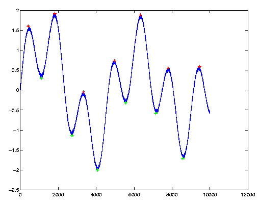
The local maxima and minima are plotted as red and green stars on the graph. To the eye it’s so obvious where they are, but making a computer find them can turn out tricky.
Let’s start with what not to do: Using the well-known zero-derivate method. Due to the noise, which is always there in real-life signals, accidental zero-crossings of the first derivate occur, yielding false detections. The typical solution is to smooth the curve with some low-pass filter, usually killing the original signal at the same time. The result is usually that the algorithm goes horribly wrong where it’s so obvious to the eye.
In many cases, we don’t really care about maxima and minima in the mathematical sense. We can see the peaks and valleys, and we want the computer to find them. This is what “peakdet” does.
The trick here is to realize, that a peak is the highest point betweem “valleys”. What makes a peak is the fact that there are lower points around it. This strategy is adopted by “peakdet”: Look for the highest point, around which there are points lower by X on both sides.
Let’s see an example: First, let’s create the graph shown in the figure above:
>> t=0:0.001:10;
>> x=0.3*sin(t) + sin(1.3*t) + 0.9*sin(4.2*t) + 0.02*randn(1, 10001);
>> figure; plot(x);
Now we’ll find the peaks and valleys: (you’ll need to copy the “peakdet” function from the bottom of this page and put it in your working directory or a directory in the MATLAB search path):
>> [maxtab, mintab] = peakdet(x, 0.5);
>> hold on; plot(mintab(:,1), mintab(:,2), 'g*');
>> plot(maxtab(:,1), maxtab(:,2), 'r*');
Note the call to peakdet(): The first argument is the vector to examine, and the second is the peak threshold: We require a difference of at least 0.5 between a peak and its surrounding in order to declare it as a peak. Same goes with valleys.
The returned vectors “maxtab” and “mintab” contain the peak and valley points, as evident by their plots (note the colors).
The vector’s X-axis values can be passed as a third argument (thanks to Sven Billiet for his contribution on this), in which case peakdet() returns these values instead of indices, as shown in the following example:
>> figure; plot(t,x);
>> [maxtab, mintab] = peakdet(x, 0.5, t);
And from here we continue like before, but note that the X axis represents “t” and not indices.
>> hold on; plot(mintab(:,1), mintab(:,2), 'g*');
>> plot(maxtab(:,1), maxtab(:,2), 'r*');
As for the implementation of this function: The work is done with a for-loop, which is considered lousy practice in MATLAB. Since I’ve never needed this function for anything else than pretty short vectors (< 100000 points), I also never bothered to try speeding it up. Compiling to MEX is a direct solution. I’m not sure if it’s possible to vectorize this algorithm in MATLAB. I’ll be glad to hear suggestions.
A final note: If you happen to prefer Python, you could try this (someone has been kind enough to convert this function). There are also a version in C by Hong Xu and a version in FORTRAN 90 by Brian McNoldy. I haven’t verified any of these.
And here is the function. Copy and save it as ‘peakdet.m’. It’s released to the public domain:
function [maxtab, mintab]=peakdet(v, delta, x)
maxtab = [];
mintab = [];
v = v(:);
if nargin < 3
x = (1:length(v))';
else
x = x(:);
if length(v)~= length(x)
error('Input vectors v and x must have same length');
end
end
if (length(delta(:)))>1
error('Input argument DELTA must be a scalar');
end
if delta <= 0
error('Input argument DELTA must be positive');
end
mn = Inf; mx = -Inf;
mnpos = NaN; mxpos = NaN;
lookformax = 1;
for i=1:length(v)
this = v(i);
if this > mx, mx = this; mxpos = x(i); end
if this < mn, mn = this; mnpos = x(i); end
if lookformax
if this < mx-delta
maxtab = [maxtab ; mxpos mx];
mn = this; mnpos = x(i);
lookformax = 0;
end
else
if this > mn+delta
mintab = [mintab ; mnpos mn];
mx = this; mxpos = x(i);
lookformax = 1;
end
end
end
I’m using MATLAB since about 1992. One of the things that I’ve always missed, as a communication engineer, is a quick and dirty spectrum plot of signals. I want to see what the spectrum analyzer will show me when I’ll run the signal through it, and not some analytic plot, which looks nothing like.
The “easyspec” MATLAB function does exactly that. Using this function on a time signal has the feel of plugging in a spectrum analyzer: You get some simple, concise image (scaled in dBs, for us engineers), which is as reliable as if you measured the signal. Meaning, that if the signal is not stationary (choose whatever sense you want for “stationary”) you may want to re-run the function to see if you get the same result.
Let’s try a simple session (you’ll need to copy the “easyspec” function from the bottom of this page and put it in your working directory or a directory in the MATLAB search path):
>> t=0:1/44100:10;
>> s=0.25*sin(2*pi*440*t) + sin(2*pi*1000*t) + randn(1,441001);
>> easyspec(s, 44100);
This shows the spectrum of two tones, one at 440Hz, and another at 1000Hz, sampled at 44.1 kHz. Note that since we hand over the sample rate to easyspec, it will show the real-life frequency on the x axis.
The special thing about this function, is that it chooses the FFT segments at random. As a result, subsequent calls to this function on the same signal will result in slightly differently plots. This is exactly what we expect from a real-life spectrum analyzer.
As given below, this function picks (at random) 100 segments of 4096 samples, applies a Hanning window to each, and pads the vector to a length of 16384. The absolute value of the FFT of this vector is calculated.
What is displayed is the average of these 100 absolute value vectors, normalized so that a sine wave of amplitude 1 will show as approximately 0 dB on the spectrum plot. This is in the spirit of the “video average” function of common spectrum analyzers, but it works differently (spectrum analyzers usually average on the dB values). Anyhow, this makes a smoother display of truly random signals (such as noise).
The most common question I get is where the 17.127 constant came from. The honest answer is that I simply played with the number until I got 0 dB for a unity sine wave. It’s true that I could have made some calculations to reach a constant with theory behind, but I found it pretty pointless, since the accuracy is compromised anyhow. (The main reason is that the reading depends on the frequency, as each FFT bin’s response to a pure sine wave is the Hanning window’s Fourier transform).
The reason for picking the segments at random comes from real-life spectrum analyzers: Almost always, there is no synchronization between the sweep instances and the measured signal. Also, let’s keep in mind that the term “spectrum” comes from the world of probability theory, and it’s the Fourier Transform of the autocorrelation function of a side-sense stationary random signal. Now we may ask ourselves what meaning there is to a spectrum of a deterministic signal. What’s random about a plain sine wave that we apply to a spectrum analyzer?
The answer is that the time segment, on which we measure the signal, is random. If it’s not, as in MATLAB’s native “spectrum” function, a misleading result may be displayed as a result of some relation between the measured signal’s periodicity and the jumps between the FFT segments. This doesn’t happen when the signal is simple noise, but as soon as there is anything periodic about it, strange things can happen.
And finally, here is the function in question. Copy and save it as ‘easyspec.m’. It’s released to the public domain:
function [s,f]=easyspec(x,fs)
if nargin==0
error('No input vector given');
end
if (nargin==1)
fs=2;
end
NFFT=16384; NWIN=NFFT/4;
LOOP=100;
win=hanning(NWIN)';
x=x(:)'*(17.127/NFFT/sqrt(LOOP));
n=length(x);
maxshift=n-NWIN;
if (n<2*NWIN)
error(['Input vector should be at least of length '...
num2str(2*NWIN)]);
end
s=zeros(1,NFFT);
for i=1:LOOP
zuz=floor(rand*maxshift);
s=s+abs(fft([win.*x(1+zuz:NWIN+zuz) zeros(1,NFFT-NWIN)])).^2;
end
s=10*log10(s(1:NFFT/2));
f=linspace(0,fs/2,NFFT/2);
if nargout==0
hold off;
plot(f,s);
ylabel('Power Spectrum [dB]');
xlabel('Frequency');
grid on; zoom on;
end
Introduction
2022 update: This is probably quite pointless today, but that’s not reason enough to delete this post.
cdepend is a cross-reference utility, whose main purpose is mapping which function calls which in a C language project.
As projects grow and develop, it becomes harder and harder to keep track of which functions are actually used. Unused functions may exist in the project without anyone noticing.
Sometimes we want to change a function, but we’re not sure how this change will affect the entire project.
Another feature of cdepend is getting details about where library functions are called. This is important when porting a project to a non-UNIX environment, where the most basic library functions may be absent.
cdepend addresses these issues. A simple example of how it’s used and the output it generates is given below.
Project status
The project works well on my own computer. If you’re running a recent i386-Linux distro, you have good chances of having it up quickly as well. If not, you may run into trouble. If you do, I will most probably help you, assuming that you’ll supply me with sufficient information. Especially if you’re running on a recent version of Linux.
Download & Install
First you’d like to download the tarball (or get it at SourceForge). Then you do something like:
[eli@localhost cdepend]$ tar -xzf cdepend-0.02.tar.gz
[eli@localhost cdepend]$ cd cdepend-0.02
[eli@localhost cdepend-0.02]$ perl Makefile.PL
Checking if your kit is complete...
Looks good
Writing Makefile for cdepend
[eli@localhost cdepend-0.02]$ make
(... snipped ...)
[eli@localhost cdepend-0.02]$ su
[root@localhost cdepend-0.02]# make install
[eli@localhost cdepend-0.02]$ man cdepend
Note that there is a man page. Read it!
Example of use
Suppose that we have two files, mainfile.c and funcfile.c.
mainfile.c goes as follows:
void f1(int);

int main() {
  f1(3);
}
and funcfile.c:
void f2(int);

void f1(int num) {
  if (num > 0)
    f2(num);
}

void f2(int num) {
  printf("Hello World %d\n", num);
  f1(num-1);
}
What these functions do is really not interesting. Just for reference, here’s how we would probably compile this “project”:
[eli@localhost example]$ gcc -c mainfile.c -o mainfile.o
[eli@localhost example]$ gcc -c funcfile.c -o funcfile.o
[eli@localhost example]$ gcc mainfile.o funcfile.o -o try
Nothing new so far. Now let’s try cdepend!
First, we have to partially compile the files: We want assembly code, not object files. So we add the -S flag. We also must have the -gstabs+ flag, so debugging information is written to the assembly files. Then we run cdepend, giving it both assembly files (*.S) as input data:
[eli@localhost example]$ gcc -S -gstabs+ mainfile.c -o mainfile.S
[eli@localhost example]$ gcc -S -gstabs+ funcfile.c -o funcfile.S
[eli@localhost example]$ cdepend -o report.txt -d funcdir *.S
The report.txt is not interesting in this case, because all functions are used and declared. It’s basically empty.
But cdepend generated a directory, funcdir at our request. Let’s see what we have in the file funcdir/f1 (generated by cdepend, of course):
Variable's name: f1()
Declared at /home/eli/example/funcfile.c:3
Varible/function is recursive (indirectly)

Functions/Variables used directly:
==================================
f2() at line(s): 5

Functions/Variables using directly:
===================================
f2() at /home/eli/example/funcfile.c:10
main() at /home/eli/example/mainfile.c:4
From this file we can learn where the function is declared, and that there is a recursive connection from f1() back to itself. Then we see that f1() is calls f2() at line 5, and that f1() is called by f2() and main().
There are similar files for f2() and main(). But we shall have a look on funcdir/printf:
Variable's name: (printf)
Found in linkable library /lib/i686/libc.so.6

Functions/Variables using directly:
===================================
f2() at /home/eli/example/funcfile.c:9
This information is important when porting a project to an environment where there is no printf. Here we can tell who uses this function.
Note that on some platforms library functions will be displayed as undeclared. This behaviour does not impact the reliabilty of the rest of the information.
And once again: There is a UNIX manual page for cdepend. man cdepend should work after installation.
Frandom is a Linux kernel random number generator, which is 10-50 times faster than what you get from Linux’ built-in /dev/urandom. And it uses very little (/dev/frandom) or none (/dev/erandom) of the kernel’s entropy pool, so it is very useful for applications that require a handy source for lots of random data.
Its most common use seems to be wiping large hard disks with random data before encryption. It’s currently supporting 2.6 kernels, but was originally written for version 2.2.
Download the kernel module tarball.
And here’s some answers to things you might ask yourself:
- Isn’t
/dev/urandom enough?
Discussions about the necessity of a faster kernel random number generator rise and fall since 1996 (that I know of). My opinion is that /dev/frandom is as necessary as /dev/zero, which merely creates a stream of zeroes. The common opposite opinion usually says: Do it in user space.
- What’s the difference between
/dev/frandom and /dev/erandom?
In the beginning I wrote /dev/frandom. Then it turned out that one of the advantages of this suite is that it saves kernel entropy. But /dev/frandom consumes 256 bytes of kernel random data (which may, in turn, eat some entropy) every time a device file is opened, in order to seed the random generator. So I made /dev/erandom, which uses an internal random generator for seeding. The “F” in frandom stands for “fast”, and “E” for “economic”: /dev/erandom uses no kernel entropy at all.
- How fast is it?
Depends on your computer and kernel version. Tests consistently show 10-50 times faster than /dev/urandom.
- Will it work on my kernel?
It most probably will, if it’s > 2.6.
- Is it stable?
Since releasing the initial version in fall 2003, at least 100 people have tried it (probably many more) on i686 and x86_64 systems alike. Successful test reports have arrived, and zero complaints. So yes, it’s very stable. As for randomness, there haven’t been any complaints either.
- How is random data generated?
frandom is based on the RC4 encryption algorithm, which is considered secure, and is used by several applications, including SSL. Let’s start with how RC4 works: It takes a key, and generates a stream of pseudo-random bytes. The actual encryption is a XOR operation between this stream of bytes and the cleartext data stream.
Now to frandom: Every time /dev/frandom is opened, a distinct pseudo-random stream is initialized by using a 2048-bit key, which is picked by doing something equivalent to reading the key from /dev/urandom. The pseudo-random stream is what you read from /dev/frandom.
frandom is merely RC4 with a random key, just without the XOR in the end.
- Does frandom generate good random numbers?
Due to its origins, the random numbers can’t be too bad. If they were, RC4 wouldn’t be worth anything.
As for testing: Data directly “copied” from /dev/frandom was tested with the “Diehard” battery of tests, developed by George Marsaglia. All tests passed, which is considered to be a good indication.
- Can frandom be used to create one-time pads (cryptology)?
frandom was never intended for crypto purposes, nor was any special thought given to attacks. But there is very little room for attacking the module, and since the module is based upon RC4, we have the following fact: Using data from /dev/frandom as a one-time pad is equivalent to using the RC4 algorithm with a 2048-bit key, read from /dev/urandom.
Bottom line: It’s probably OK to use frandom for crypto purposes. But don’t. It wasn’t the intention.
Eobj is a Perl programming environment. Well, technically speaking, it’s a Perl module. Eobj stands for Easy Objects.
Idea: Object oriented programming is supported very well in Perl, but it requires some rather advanced programming techniques: Perl modules and namespaces, references, blessings and some syntactic sugars. In addition, the awareness of some special variables is required.
Eobj is intended to bring object oriented programming to the layman Perl programmer’s doorstep. “Object oriented for dummies”, if you like. It supports an easy way to create classes, and a comfortable to handle object’s properties (a.k.a. member variables). The code looks clean, and is easy to understand, even if you’re not so good in Perl.
Most of the criticism I’ve gotten regarding Eobj is that I’ve done things differently from Java and C++. That only makes me feel better. Others claim that Eobj is not needed. Those who say that usually know more than ten ways to access a referenced hash. Most Perl programmers don’t want to know what a reference is. And I understand them.
For someone who understands the basic principles of object oriented programming and “normal” Perl script programming, it should take no longer than 15 minutes before being able to get started. There are a few quite simple rules to follow, and off you are.
Almost all features of “classic” Perl OO programming is supported. The main cost of using Eobj is some overhead. But if you’re worried about memory and speed, why are you using Perl?
Eobj is derived from the Perlilog project. In fact, Perlilog’s object environment is very similar to Eobj’s, there are minor differences. Eobj is intended as a general-purpose environment, while Perlilog’s object environment is adapted to its certain purpose.
Eobj is released on CPAN, and can be downloaded from any of its mirrors. In particular, it’s available at http://search.cpan.org/~billauer/ (you may browse the manual page at http://search.cpan.org/~billauer/Eobj-0.23/Eobj.pm)
Somewhere in 2006 TI (Texas Instruments) released a clock synthesizer, CDCE906, which is pretty much everything one can look for in a system clock generator: Several (up to 6) clock outputs derived from a single reference clock or crystal with excellent multiplication and division capabilities, not to mention low jitter, slew rate control, spread spectrum and more. On top of all, it’s surprisingly low-priced. So it’s a chip you want to consider, even if all you (think you) need for now, is one single system clock with a fixed frequency. It will save you, when you’ll discover three weeks before release that you actually need another clock with a weird frequency. Believe me.
Except for the non-E devices, (that is, CDC906 and CDC706, which TI seems to neglect) the devices’ setting can be preprogrammed into an on-chip EEPROM, before or after the chip is put on the PCB board. If this is enough for you, frankly, you have nothing to look for on this page. On the other hand, if you want to set the current configuration regardless of the EEPROM, it’s possible over the SMBus.
Now, SMBus is more or less like I2C (also known as IIC), so if you have a controller on the board with I2C/SMBus cababilities, you may want to use it (if it has I2C, I suggest knowing the differences). If there is no controller around, or you prefer the FPGA to set up the synthesizer, the Verilog code below is what you need.
It should be pointed out, that TI also have another very similar device, CDCE706, which is surprisingly enough more capable than its “little brother” CDCE906. Their register structure is identical however, so the code below can be used for CDCE706 as well.
The only downside about both devices is that being very versatile, they’re also complicated. I’m not going to describe how to run these chips. There is no way out of reading the extensive datasheet, and I promise finding some hidden treasures there. The only thing this module will do for you, is get the right values to the right register.
So let’s get to business. Before doing anything else, be sure to set the parameter “clk_freq” to the frequency of the module’s input clock “clk” (in MHz, nearest integer). This is crucial, because the SMBus is derived from this clock. If several frequencies are possible, make “clk_freq” the highest one.
Important notes:
- Pullup resistors for sclk and sdata are mandatory. Nothing will work without them. When tied to a 3.3V supply, they should be between 10 kOhm and 33 kOhm.
- This module acts as an SMBus master. It must therefore not share the sclk and sdata lines with another master, unless it’s assured that they won’t attempt to take control at the same time. The simplest solution is to make one-on-one connections of sclk and sdata between the chip and the FPGA (don’t forget the pullups!).
- Verify that the FPGA outputs are indeed 3.3V (this is usually something you should set). Modern FPGA’s take a lower voltage by default.
Now the basic I/O’s:
| clk |
Input clock, which drives the module’s logic and from which the SMBus clock is derived. Preferably with a known and stable frequency. The module is sensitive to this clock’s rising edge only. |
| reset |
Asynchronous reset, active high (input). May be tied to ’0′ if the state variable “state” can be assured to wake up as “st_idle” (don’t trust the syntheizer to do this implicitly) |
| send_data |
Input, synchronous with “clk”: Start send data to chip command. Set to ’1′ to update all registers of the chip. This line should be ’1′ for at least one “clk” cycle, but not more than the time it takes for the full write to complete. |
| busy |
Output, synchronous with “clk”: This line is high as long as the register data is being written to the chip over the SMBus. |
| error |
Output, synchronous with “clk”: This line goes high if an acknowledgement from the chip is missing, which indicates some kind of error. The line remains high until the next initiation with “send_data”. |
| sclk |
Output: To be directly connected to the chip’s pin #10 (SCLOCK). This pin toggles between ’0′ and high-Z. Do verify that your development tools indeed create a high-Z condition on the output when the ‘z’ value is assigned to this line (Xilinx FPGA tools are OK with this). Don’t forget the pullup resistor |
| sdata |
Output: To be directly connected to the chip’s pin #9 (SDATA). This pin toggles between ’0′ and high-Z. Do verify that your development tools indeed create a high-Z condition on the output when the ‘z’ value is assigned to this line. Don’t forget the pullup resistor |
| S0 |
Output: To be directly connected to the chip’s pin #1 (S0/A0/CLK_SEL). Will be tied to constant ’1′ (see datasheet for meaning). |
| S1 |
Output: To be directly connected to the chip’s pin #2 (S1/A1). Will be tied to constant ’1′ (see datasheet for meaning). |
Next we have the actual synthesizer parameters, whose meaning should be obvious to whoever has read the datasheet well. The only thing note is that the term “PLL” has been exchanged for “VCO”, which I find more intuitive. So VCO1_M and VCO1_N are the M and N for PLL1, using the datasheet’s terminology, etc. The comments in the module itself may help as well.
All these inputs can be constants (which will shrink the synthesized logic) or you can wire them to whatever you like, but these inputs must be steady as long as their content is flushed to the chip ( = as long as the “busy” output is high).
So all we have left is the module itself. I’ve lifted the copyright restrictions for it, so you can use it in any way you like.
(And by the way: I have no special relations with TI whatsoever. Not even as a freelancer).
———————————–
module cdce906
(
clk, reset, send_data,
busy, error,
sclk, sdata, S0, S1,
VCO1_M, VCO1_N, VCO1_bypass, VCO1_hi_freq_range,
VCO2_M, VCO2_N, VCO2_bypass, VCO2_hi_freq_range,
VCO3_M, VCO3_N, VCO3_bypass, VCO3_hi_freq_range,
P0_VCO_select, P0_div, P1_VCO_select, P1_div,
P2_VCO_select, P2_div, P3_VCO_select, P3_div,
P4_VCO_select, P4_div, P5_VCO_select, P5_div,
Y0_en, Y0_inv, Y0_slew_rate, Y0_div_select,
Y1_en, Y1_inv, Y1_slew_rate, Y1_div_select,
Y2_en, Y2_inv, Y2_slew_rate, Y2_div_select,
Y3_en, Y3_inv, Y3_slew_rate, Y3_div_select,
Y4_en, Y4_inv, Y4_slew_rate, Y4_div_select,
Y5_en, Y5_inv, Y5_slew_rate, Y5_div_select,
SSC_mod_select, SSC_freq_select
);
input clk;
input reset;
output sclk;
inout sdata;
output S0, S1;
output busy, error;
input send_data;
input [8:0] VCO1_M;
input [11:0] VCO1_N;
input VCO1_bypass;
input VCO1_hi_freq_range;
input [8:0] VCO2_M;
input [11:0] VCO2_N;
input VCO2_bypass;
input VCO2_hi_freq_range;
input [8:0] VCO3_M;
input [11:0] VCO3_N;
input VCO3_bypass;
input VCO3_hi_freq_range;
input [2:0] P0_VCO_select;
input [6:0] P0_div;
input [2:0] P1_VCO_select;
input [6:0] P1_div;
input [2:0] P2_VCO_select;
input [6:0] P2_div;
input [2:0] P3_VCO_select;
input [6:0] P3_div;
input [2:0] P4_VCO_select;
input [6:0] P4_div;
input [2:0] P5_VCO_select;
input [6:0] P5_div;
input Y0_en;
input Y0_inv;
input [1:0] Y0_slew_rate;
input [2:0] Y0_div_select;
input Y1_en;
input Y1_inv;
input [1:0] Y1_slew_rate;
input [2:0] Y1_div_select;
input Y2_en;
input Y2_inv;
input [1:0] Y2_slew_rate;
input [2:0] Y2_div_select;
input Y3_en;
input Y3_inv;
input [1:0] Y3_slew_rate;
input [2:0] Y3_div_select;
input Y4_en;
input Y4_inv;
input [1:0] Y4_slew_rate;
input [2:0] Y4_div_select;
input Y5_en;
input Y5_inv;
input [1:0] Y5_slew_rate;
input [2:0] Y5_div_select;
input [2:0] SSC_mod_select;
input [3:0] SSC_freq_select;
reg SMBus_en, pre_en;
reg kickoff;
reg [2:0] state;
reg get_bit;
reg next_bit, this_is_ack, wait_for_ack;
reg sdata_d;
reg error;
reg [4:0] word_addr;
reg [3:0] bit_pos;
reg no_more_bits;
reg [7:0] SMBus_word;
reg [11:0] div_counter;
reg sclk_logic, sdata_logic;
parameter clk_freq = 10;
parameter st_idle = 0,
st_start0 = 1,
st_start1 = 2,
st_bit0 = 3,
st_bit1 = 4,
st_bit2 = 5,
st_stop0 = 6,
st_stop1 = 7;
assign sclk = sclk_logic ? 1'bz : 1'b0 ;
assign sdata = sdata_logic ? 1'bz : 1'b0 ;
assign S0 = 1;
assign S1 = 1;
always @(posedge clk)
begin
SMBus_en <= pre_en;
sdata_d <= sdata;
if (div_counter == ((clk_freq * 10) - 1))
begin
div_counter <= 0;
pre_en <= 1;
end
else
begin
div_counter <= div_counter + 1;
pre_en <= 0;
end
end
always @(posedge clk or posedge reset)
if (reset)
kickoff <= 0;
else if (send_data)
kickoff <= 1;
else if (SMBus_en)
kickoff <= 0;
assign busy = kickoff || (state != st_idle);
always @(posedge clk or posedge reset)
if (reset)
begin
state <= st_idle;
error <= 0;
end
else if (SMBus_en)
case (state)
st_idle: begin
sclk_logic <= 1;
sdata_logic <= 1;
get_bit <= 0;
if (kickoff)
state <= st_start0;
end
st_start0: begin
sclk_logic <= 1;
sdata_logic <= 0;
state <= st_start1;
error <= 0;
end
st_start1: begin
sclk_logic <= 0;
state <= st_bit0;
end
st_bit0: begin
sclk_logic <= 0;
sdata_logic <= next_bit;
wait_for_ack <= this_is_ack;
get_bit <= 1;
state <= st_bit1;
end
st_bit1: begin
sclk_logic <= 1;
get_bit <= 0;
state <= st_bit2;
end
st_bit2: begin
sclk_logic <= 0;
if (wait_for_ack && !sdata_d && !kickoff)
state <= st_bit2;
else if (no_more_bits)
state <= st_stop0;
else
state <= st_bit0;
if (wait_for_ack && sdata_d && sclk_logic)
error <= 1;
end
st_stop0: begin
sclk_logic <= 0;
sdata_logic <= 0;
state <= st_stop1;
end
st_stop1: begin
sclk_logic <= 1;
state <= st_idle;
end
endcase
always @(posedge clk)
if (SMBus_en)
begin
if (kickoff)
begin
word_addr <= 0;
bit_pos <= 7;
no_more_bits <= 0;
end
else if (get_bit)
begin
bit_pos <= (bit_pos == 0) ? 8 : bit_pos - 1;
if (bit_pos == 0)
word_addr <= word_addr + 1;
if ((word_addr == 29) &&
(bit_pos == 8))
no_more_bits <= 1;
end
if (bit_pos == 8)
begin
next_bit <= 1;
this_is_ack <= 1;
end
else
begin
next_bit <= SMBus_word[ bit_pos[2:0] ];
this_is_ack <= 0;
end
end
always @(posedge clk)
if (SMBus_en)
case (word_addr)
0: SMBus_word <= 8'b1101001_0 ;
1: SMBus_word <= 0 ;
2: SMBus_word <= 26 ;
3: SMBus_word <= 0 ;
4: SMBus_word <= VCO1_M[7:0] ;
5: SMBus_word <= VCO1_N[7:0] ;
6: SMBus_word <= { VCO1_bypass, VCO2_bypass, VCO3_bypass, VCO1_N[11:8], VCO1_M[8] } ;
7: SMBus_word <= VCO2_M[7:0] ;
8: SMBus_word <= VCO2_N[7:0] ;
9: SMBus_word <= { VCO1_hi_freq_range, VCO2_hi_freq_range,
VCO3_hi_freq_range, VCO2_N[11:8], VCO2_M[8] } ;
10: SMBus_word <= VCO3_M[7:0] ;
11: SMBus_word <= VCO3_N[7:0] ;
12: SMBus_word <= { P0_VCO_select, VCO3_N[11:8], VCO3_M[8] } ;
13: SMBus_word <= { P1_VCO_select, 1'b0, 2'b00, 2'b00 } ;
14: SMBus_word <= { 2'b00, P3_VCO_select, P2_VCO_select } ;
15: SMBus_word <= { 2'b00, P5_VCO_select, P4_VCO_select } ;
16: SMBus_word <= { 1'b0, P0_div } ;
17: SMBus_word <= { 1'b0, P1_div } ;
18: SMBus_word <= { 1'b0, P2_div } ;
19: SMBus_word <= { 1'b0, P3_div } ;
20: SMBus_word <= { 1'b0, P4_div } ;
21: SMBus_word <= { 1'b0, P5_div } ;
22: SMBus_word <= { 1'b0, Y0_inv, Y0_slew_rate, Y0_en, Y0_div_select } ;
23: SMBus_word <= { 1'b0, Y1_inv, Y1_slew_rate, Y1_en, Y1_div_select } ;
24: SMBus_word <= { 1'b0, Y2_inv, Y2_slew_rate, Y2_en, Y2_div_select } ;
25: SMBus_word <= { 1'b0, Y3_inv, Y3_slew_rate, Y3_en, Y3_div_select } ;
26: SMBus_word <= { 1'b0, Y4_inv, Y4_slew_rate, Y4_en, Y4_div_select } ;
27: SMBus_word <= { 1'b0, Y5_inv, Y5_slew_rate, Y5_en, Y5_div_select } ;
28: SMBus_word <= { 1'b0, SSC_mod_select, SSC_freq_select } ;
default: SMBus_word <= 0 ;
endcase
endmodule
Perlilog is a command-line tool which generates Verilog modules from a set of files, which come in several other formats. It was originally designed to integrate Verilog IP cores. It’s released as free software (GPL).
Motivation: Anyone who has needed to integrate a few Verilog modules into something working, knows it’s a headache. It’s not only a mechanic task, but also a source of bugs. Since Verilog modules’ interface is basically wires, the integration task requires an accurate understanding of what each wire stands for, and how it’s expected to behave. Having many details to keep track on, it’s common that undesidered
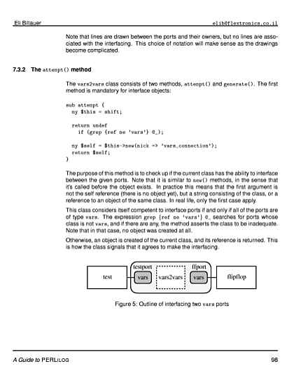
Perlilog’s main concept is that handling IP cores (and Verilog modules in general) should be intuitive. We think about IP cores as black boxes, so we should also relate to them as black boxes when connecting them. When connecting cores, we imagine that as drawing a thick line between them. So should the connection be done, when actually integrating the system.
Perlilog introduces an alternative concepts for connecting between cores. The main issues are:
- Rather than connecting wires (Verilog inputs and outputs), connect ports. A port is a loosely defined object, which holds one simple rule: Connecting port A with port B should mean what one would normally expect from drawing a line between two blocks in a schematic block diagram. Surprisingly enough, it’s almost always possible to properly define this meaning.
- Cores should be black boxes, and they must be easy to configure. The meaning of each attribute should be obvious (as opposed to editing define files)
Perlilog is also useful for much simpler tasks, such as massive connection of Verilog module’s inputs and outputs to pads, and other tasks that are readily performed with Perl scripts. It’s a good starting point for writing a Perl script which handles Verilog code, even for the simpler tasks (and hence the project’s name, as a “mixture” between Perl and Verilog).
Most Linux distributions have Perlilog packaged, so the easiest way to obtain it is with yum, apt-get, or whatever applies. Or you may download the project and its guide or directly from this site: Perlilog-1.0.tar.gz and perlilog-guide-1.0.pdf.
Since I’ve cleaned up the site a bit, there were a few pages that fit nowhere, so this pseudo-post contains links to them, or else they might become unreachable for search engine crawlers. So:
Ehm.. This is really outdated
Cinelerra has made a long way since this was written. So really, take this with a grain of salt.
Making the Dyne::Bolic live CD feel at home
- Nest (under /dyne). 128 MB should be enough
- Dock
- Boot from hard disk
- Make a swap partition (if it exists, it will be used automagically)
Starting a project
- Start up cinelerra from fresh
- Set the desired output format wisely (Settings->Format…). If you have a trancoder utility (e.g. mencoder), the most used input format is preferred. You are going to transcode the output to the target format afterwards anyhow.
- Set the frame rate. Changing it later may disrupt A/V sync.
- No less important: Check the resources’ info (right-click the video file’s entry in the resource in the resource window) and make sure that the frame rate matches the real frame rate exactly. A bug in Cinelerra may change this value slightly, causing A/V sync problems during rendering.
- Set the video track(s) size to match the output’s: Right-click the video track and pick “Match output size” (or “Resize track…”). This is important in particular when editing PAL videos.
- Load the video/audio files (File->Load files). “Create new resources only” is preferred. Take them all at once, since this can take time.
- … but not too many: If Cinelerra crashes, take them a few at a time.
- Set the preferences NOT to play every frame (Settings->Preferences->Playback->Video Out->Play every frame unchecked).
- Also consider turning off Settings->Preferences->Playback->Audio Out->View follows playback if the video playback freezes often.
- Save your project file (File->Save As…)
Input formats
- Rule #1: Don’t lose your sanity
- Cinelerra isn’t very friendly in this respect, but formally supports most things you’d like to import. Nevertheless, it’s very sensitive to quirks in the stream.
- MPEG-2 (the format used in DVDs) is OK, but only for short clips (four minutes?) or A/V sync is slowly lost.
- AVI/DIVX seems to be a good format for import
- When using mencoder to create an input file, always use the
-vf harddup option, so duplicate frames are explicitly coded in the stream. Failing to do so will make some keyframed effects go crazy. This is important in particular when changing the frame rate.
- MJPEG works well. mencoder can be used for recoding (keep in mind that MJPEG involves some flicker noise):
mencoder input_file.avi -oac mp3lame -ovc lavc -vf harddup -lameopts abr:q=5 -lavcopts vcodec=mjpeg -ffourcc MJPG -o output_file.avi
- Videos marked as “divx” (as opposed to “DIVX”) are not recognized.
- MPEG-2 is accepted, but a TOC file is generated in the .bcast directory, and that takes time.
- Better alternative (when it works):
mpeg3toc -v /path/to/video.mpg video.toc Always make the path absolute, since this path is written in the TOC file. Then load the .toc file (not the .mpg) to Cinelerra.
- To get an MPEG-2 file from DVD track 1:
mencoder dvd://1 -dvd-device /dev/scd0 -vf harddup -oac copy -ovc copy -of mpeg -mpegopts format=dvd -o video.mpg
(Note that -dvd-device should point at your DVD player)
- For really long MPEG-2′s, concatenating VOBs (with “cat”) is safer.
- Other MPEG flavors should be OK as well (haven’t tried)
- MJPEG from a Canon S3 camera works 100%
Two-screen editing
- Browse through the media in the Viewer. Find the juicy snippets and send them into the timeline or make clips
- See what you got in the Compositor
- Labels are very useful for navigating in the timeline
- Except for time jumps, what you see in the Compositor is what you’ll get.
Editing by draggin handles
- In “Cut and Paste mode” (“I” toolbar button pressed), dragging the beginnings or ends of edits.
- Only armed tracks are affected
- With left button, edits are shortened or extended the overall time changes
- With middle button, only the cut time changes, one edit “stealing” time from the other.
- With right button, overall time is not changed, but media is shifted in the opposite direction of the drag direction. In effect, you mark the beginning or end of the edit, and it’s shifted to match that.
- These are default mouse button settings, and can be changed.
Arming
- The red button
- Shift-click for arm one track only or all tracks
Add an image
- Due to a bug in Version CV 2.1 (and probably others), this doesn’t work at all when the frame rate divided by 3 is an integer (or so it seems). Avoid the frame rate 30 (as opposed to 29.97)
- Transparency is respected. Use it (in PNG images).
- … but if there is nothing behind the transparent image, the background becomes white (or black. Or anything)
- Load the image file as a resource
- Create a video track
- Select entry poiny in timeline
- Zoom in timeline, so that one frame period is viewable
- Disarm all tracks, arm the new track
- Drag the image into timeline or right-click-paste on resource
- Zoom out timeline and extend the duration of the image using edit dragging
- See my bug report: CV version bug #459
Effects
- Translate
- Chroma Key / Difference Key
- ReframeRT (slow motion / crazy motion)
- Reroute (future versions)
- Effects work on a single track
- … unless they are explicitly shared
Rendering
- Close the compositor video, if you don’t want to watch the rendering process. (May slow down rendering significantly)
- DO NOT RENDER TO AVI. Use Quicktime for Linux instead.
- Heavy A/V sync problems have been experienced when rendering to AVI
- To get a DIVX: Use MP3 audio compression (256 kbits?) and MPEG-4 Video with default parameters.
- Then convert to AVI:
mencoder clip.mov -oac mp3lame -ovc copy -ffourcc DIVX -o clip.avi
- Re-encoding to DIVX is advisable to be sure to get a clean file.
- If A/V sync problems occur, render audio and video separately, and then multiplex. mencoder’s
-audiofile parameter may come handy.
- Note that it’s “DIVX”, not “divx”
Rendering for DVD
- Video and Audio are rendered separately
- MPEG-2 streams can be generated directly from Cinelerra, but the manual doesn’t tell you to do that.
- … maybe because it’s easy to get off-standard with many GUI parameters to set.
- For video, the output file format is YUV4MPEG, and check “To Pipe”.
- Create an executable script (with #!/bin/bash) file saying:
mpeg2enc -v 0 -K tmpgenc -r 16 -4 1 -2 1 -D 10 -E 10 -g 15 -G 15 -q 6 -b 8600 -f 8 -o /path/to/output-video-file.m2v
- Note that unlike what’s implied in the manual, Cinelerra doesn’t pass the output file name as first argument to the script. The file name is therefore hardcoded
- It does send some garbage instead. A simple trick is to end the pipe’s command with a ‘#’ which comments out the garbage
- Then choose AC3 as output format, and render audio. The standard allows up to 1536 kBits/sec, so you can’t go wrong with this.
- Note that you can use mencoder and YUV4MPEG as well for a “safer” encoding.
- Check the console for error messages and progress (when using mencoder)
- When using mencoder, create a raw PCM audio file (Microsoft WAV is fine) and then apply the file with the -audiofile parameter.
- In the script file you’ll have something like:
mencoder -audiofile "full/path/to/only-audio.mov" -oac lavc -ovc lavc -of mpeg -mpegopts format=dvd -vf scale=720:480 -srate 48000 -af lavcresample=48000 -lavcopts vcodec=mpeg2video:vstrict=1:vrc_buf_size=1835:vrc_maxrate=9800:vbitrate=5000:keyint=18:acodec=ac3:abitrate=192:aspect=4/3 -ofps 30000/1001 -o "movie.mpg" - (NTSC)
- Note the dash, telling mencoder to read from standard input
- If mencoder complains that it “cannot seek backward in linear streams” and “seek failed” (several times), adding the
-cache 8192 parameter is likely to help.
General remarks
- Cinelerra crashes a lot. Save your project file frequently.
- Actually, it’s recommended to save, quit and restart every 15 minutes or so (until you learn how to avoid messy situations).
- Like any typical video application, Cinelerra is pretty buggy.
- Not a single byte of media is written until you render. All edits are merely pointers to existing media
- … therefore, never move, change or delete the media files, once loaded to Cinelerra.
- Cinelerra creates backup.xml index files (and other things in) ~/.bcast
- The *.rc files in ~/.bcast are the defaults for plugins. When these are getting annoying, remove this directory between Cinelerra sessions
- DO NOT render output AVI files
- Always have Settings->Align cursor on frames checked when editing video
- Do not use Copy/Paste/Cut/Delete as you usually would in a text document. They will appear to work, but trouble will soon come. Use two-screen editing functions, drag handles or completely remove tracks instead.
- … except for copy-pasting a piece into a fresh, second Cinelerra instance for integrating several scenes to a movie (or just cleaning up the environment).
- In/out points can be applied on the main timeline. This can be used to create a clip or render a part of the full video, but be sure to remove these when not used. In particular, inserting material from the Viewer can fail (due to a bug) if In/Out points are marked on the timeline (as opposed to In/Out points on the Viewer, which you can’t without).
- Having too many “resources” (assets, things in your media list) can make Cinelerra unable to load new ones. Cinelerra keeps up to four file handles open for each, so when attempting to load another one, Cinelerra hangs and an error message misleadingly implying that the file is missing may appear at console.
- In the EDL (that is, the XML file containing edits), the timeline is given in integer frames for video edits, transitions and keyframes, based upon the expected output frame rate. This means that changing the output frame rate will cause some inprecision (in particular 30 to 29.97).
- Same applies for output audio sample rate with respect to audio edits etc.
- Output with alpha channels (transparency) is possible, for example as Quicktime for Linux with Uncompressed RGBA, or PNG output sequence. If the overall rendered image has some transparency to it, that will be reflected in the output’s alpha channel. There are only two things to note: One is that sometimes a black and completely transparent image must be put at the bottom of the timeline (master background) or elements, which should have been transparent or faded away show up. The second issue is that if non-normal overlay is used (such as multiplication overlay), the alpha channel will be set to opaque at the output.
Video formats (more…)
- For intermediate video output: Use Quicktime For Linux / Uncompressed RGB