Introduction
Ask an VLSI engineer if the Verilog “initial” keyword is legit for synthesis, and flames of fury will go your way. However in the FPGA world, it’s a portable way to assign registers and array with the initial (and possibly constant) values immediately after configuration.
The main argument against this practice is that a “real” reset should be used to set the initial values. This is a valid argument, in particular when the clock may be unstable after configuration is done. However it’s often desired to have some kind of reset-generating logic that kicks off immediately after configuration, and this way or another, it depends on the initial wakeup state. Which must be nailed down somehow.
So I made a little survey among the synthesis tools that are relevant for my own work, to verify that it’s safe to use “initial” for this purpose. The answer is yes, in short: The “initial” block is the portable way in Verilog. The references for this conclusion are given below.
Initializing registers
So, is this fine?
reg [7:0] myreg;
initial myreg = 12;
- Xilinx XST: Yes. Table 7-26 simply says that “All Initial Blocks” are supported in the XST User Guide. An example for initialing an FSM’s state variable is given in “Finite State Machines Coding Examples”. Another example is given in “Specifying INIT Value for a Flip-Flop Coding Examples”. There are also examples of initializing an array by individually setting its entries in this guide.
- Vivado: Yes, however not said explicitly in the UG901 User Guide. But given the examples showing how to initialize arrays with initial blocks, initializing plain registers go without saying (?).
- Quartus: Yes. From Chapter 8 of Quartus II Handbook, volume I, Integrated Synthesis: “The software also synthesizes variables
that are assigned values in Verilog HDL initial blocks into power-up conditions.”
Initializing an array
And what about this?
reg [3:0] mem[0:1023];
initial $readmemh("data.hex", mem);
- Xilinx XST: Yes. The XST User Guide says in the section named “Verilog System Tasks and Functions Supported in XST”: “The $readmemb and $readmemh system tasks can be used to initialize block memories”. An example for this is given in the section named “Initializing RAM From an External File”.
- Vivado: Yes. Xilinx’ User Guide UG901 in “Specifying RAM Initial Contents in an External Data File” shown an example.
- Quartus: Yes. From Chapter 8 of Quartus II Handbook, volume I, Integrated Synthesis: “Quartus II integrated synthesis supports the $readmemb and $readmemh system tasks to initialize memories”
Introduction
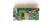
I purchased a HiTech Global 3-Port USB 3.0 SuperSpeed FMC Module (also known as USB3 FMC), which is an FPGA Mezzanine Card, primarily based upon TI’s SuperSpeed USB 3.0 Transceiver, TUSB1310A. Even though this board works fine at the end of the day, my experience with it was full with surprises, not all of which were helpful. But first:
Don’t connect the USB/FMC board to the FPGA board before reading through this post. There’s a good chance that the FPGA board will feed the board’s 1.8V power supply with 2.5V, which can potentially damage the USB board permanently. More about that below.
The board has three USB 3.0 connectors, two of which are connected to TUSB1310A transceivers, and one going to a GTX transceiver on the FPGA board. The two photos below show the front and back side of the board. I’ve made the red and green dot markings on the USB Micro-B connectors. The red dot marks the useless connector (explained below), the green one is the one that can be used, and goes to the TUSB1310A. The one not marked is connected directly to the GTX (and is useful, albeit with a few issues).
Click to enlarge photos:


A few minor irritations
These are a few issues that aren’t all that important each by itself, but they mount up. So let’s have them listed.
- The schematics isn’t available until you purchase the board.
- When the package arrived, there was a note telling me to contact support for getting the “product’s documentation for electronic delivery”, as this is an “easy and efficient mechanism for updating the reference designs, user manuals, and other related documents”. What I got was a pdf file with the schematics. That’s it. Meaning, that I had to get the FMC’s pinout from the schematics file. No text-based file (let alone an XDC file for KC705, for example), no user guide, nothing. It’s not just a waste of time to do this manually, but a source for human errors.
- It says (as of writing this) that a USB3 cable is included, but none was. USB 3.0 Micro-B connectors are different from USB 2.0, so if you’re ordering the board, be sure to acquire a cable as well.
- Their rate for shipping & handling was $100. This is just annoyingly high, being roughly twice the commonly required amount. And to be fair about it, there was an alternative method for reducing the shipping costs, which required taking care of the logistics myself. Not really important, but nevertheless annoying.
The FMC VADJ supply voltage
The board’s main power supply is VADJ_FMC, which is connected to the 1.8V power net through a 0 Ohm resistor. VADJ_FMC, as its name implies, is an adjustable voltage, generated by the FPGA board. All Xilinx boards I’m aware of have this voltage set to 2.5V by default. So whoever doesn’t pay attention to this issue, connects several components’ VDD-1.8V to 2.5V. Those of the USB transceivers and clock oscillators, that is.
It would, of course, have been much safer to use the standard 3.3V FMC power supply pins (3P3V, the voltage is standardized), and convert it to 1.8V by means of a DC/DC converter on the board, exactly as the board’s 1.1V supply is generated. It wouldn’t solve the voltage incompatibilities of the I/O connections, but there’s a difference between 2.5V on the power supply and 2.5V on the I/O wires.
Either way, there’s no user manual to warn about this, and no warning note in the schematics. Given the risk to literally blow $800, a piece of paper with a warning written in red, when you open the package, is common practice. There was nothing of this sort.
Even though “VADJ” is an “adjustable voltage”, it doesn’t mean it’s easy to adjust it. As this voltage is generated by a sophisticated power supply controller on all Xilinx’ FPGA boards, it requires reprogramming one of these controllers via PMBUS (which is an I2C-like interface). There are, in principle, two ways for doing this:
- Attaching a USB/PMBUS adapter (available from TI) and programming the power supply with TI’s GUI tool for Windows, Fusion Digital Power. The adapter isn’t expensive ($75 as of writing this), so you probably want to purchase one along with the HTG board.
- Accessing the power supply controller from the FPGA itself. I’ve written a post on this. Doesn’t require purchasing anything, but it may take quite some effort to set it up. Not recommended.
Regardless of the what way chosen, it involves changing one of the many voltages generated on the FPGA board. Depending on how bad you consider blowing the FPGA board to be, you probably want to spend some time getting acquainted with the power supply controllers, which one controls which voltage etc. No matter how you twist and turn it, you’re one little human error away from feeding the FPGA’s core voltage with 12V.
My post on this will probably help, even though it contains a lot of details that aren’t relevant for the recommended GUI tool + adapter route.
To sum this up: VADJ must be set to 1.8V on the FPGA board before the HTG is attached to the FPGA board with the FMC connector. It takes 5 minutes to do this, once you have the USB adapter at hand, the GUI tool installed and running, and the knowledge of exactly which power rail of which controller, at what PMBUS address it answers to.
One TUSB1310A path is (probably) useless
The board has two ports that are connected to TUSB1310A devices, which are in turn connected to the FMC interface. However if the board is attached to any of Xilinx’ primary development kits, KC705, KCU105 or ML605, only one of these ports can be used. I haven’t checked with other FPGA boards, but I’d expect the situation to be the same. Or maybe the second port can be used for USB 2.0 only. I had no interest in the USB 2.0 part, so I didn’t bother to check.
The problem is that not all FMC pins are connected to the FPGA on these FPGA boards: On KC705 and KCU105, neither boards have the FMC connector’s E21-E37 and F21-F37 pins connected to the FPGA, which are used for the PIPE signals on behalf of the USB port connected to J1 (with prefix P2_* on the relevant signal names in the schematics).
As for ML605, it has almost all FMC connections wired, except for four: FMC pins F37, F38, E36 and E37, which are HB20/HB21_P/N. HB20_P/N are assigned to P2_POWER_DOWN0/1 on the HTG board. These pins are disconnected (floating) on ML605. As they are lacking pulldown resistors, neither physically on the board nor by the chip itself, these wires that control the overall power state of the MGT are left floating. So ML605 can’t be used either.
Maybe there is an FPGA board out there that can use both USB ports. Still to find it.
No GTX reference clock
Even though there is a pair of signals intended as a GTX reference clock, GB_CLK_P/N, this clock pair carries no signal. The reason is that the oscillator that produces this 156.25 MHz reference clock, U9, is an TI LMK61E2 with LVPECL output. Unfortunately, the mandatory termination resistors between the LVPECL output and the capacitors are missing. As a result, the LVPECL outputs (BJT transistor’s emitters, current going only one way) just charge the capacitors, with no route to discharge them, so there’s no voltage swing, and hence no clock signal.
The obvious workaround is to use another reference clock, hopefully available on the FPGA board (on KC705 I went for the SGMII ref clock at 125 MHz, pins G7/G8).
By the way, the other identical clock oscillator, U5, generates a clock which is available as four differential clocks on the FMC interface, none of which is classified as an MGT clock on the FMC pinout, so odds are that these aren’t wired to the GTX reference pins on any FPGA board. U5 feeds a clock distributor, U9, which is a Microchip SY89833L without any capacitors in the middle. The latter chip has LVPECL-compatible inputs and LVDS outputs, so there is no problem there. It’s just not helpful for the GTX case. For general-purpose use, they are available as CLKo/1_M2C_P/N.
Design errors with the GTX data path
The board’s third USB port, J3, is intended for a direct connection with the FPGA’s GTX via one of the FMC’s dedicated gigabit pins pairs. There are a few issues to be aware of however:
First, the wire pairs are flipped in polarity in both directions (TX and RX), something that is quite apparent when looking on the FMC connector’s wiring. For example, P3_USB30_SSTX_N is connected to DP0_C2M_P. This is quite harmless, since the GTX has RXPOLARITY and TXPOLARITY ports, which can be asserted to to compensate for this error. And the USB 3.0 spec requires that both sides tolerate an P/N flip. And yet, it’s confusing to see the data stream received by the GTX without knowing about this.
Second, capacitors: There are 100 nF capacitors on the receiving wires of J3 (e.g. P3_USB30_SSRX_N) which shouldn’t be there. The standard for USB 3.0, as well as several other protocols, is that the capacitors are on the transmitting side only. Whoever designed the board knew that, because the capacitors of J1 and J2 are placed correctly (on P{1,2}_USB30_SSTX_{N,P} only).
There is a similar issue with the reference clock that is generated for the gigabit transceiver, GB_CLK_P/N: In this case, there are capacitors on the HTG board as well as the FPGA board. This isn’t really a mistake, because there is no standard on which side should put the capacitors, so both sides played safe. And this doesn’t matter, as this reference clock is dead anyhow, as mentioned above.
Putting two 100 nF capacitors in series yields an equivalent capacitor of 50 nF. For the P3_USB30_SSRX_{N,P} wires, this takes capacitance below the minimum allowed per spec, which is 75 nF. This will hardly have any effect on the gigabit data transmission, but may influence the receiver detection mechanism, which measures the current response to a voltage step. Even though a properly designed USB link partner shouldn’t be this fussy.
And one can always fetch the stereoscope and soldering iron, and replace C10 and C11 with 0 Ohm resistors.
By the way, on KC705, KCU105 (and probably all other Xilinx development kits) they’ve placed 100 nF capacitors on the receiving side only of the SMA GTX connectors (the PCIe fingers are done properly, of course). So trying to connect the USB 3.0 wires to the SMA connectors will not work, unless 100 nF capacitors are added in series with the FPGA’s transmission signals. Go figure.
The XCF constraints for KC705
Since I have it, these are the placement constraints for a KC705, as I figured them out from the schematics of the USB board and Xilinx’ reference XCF for the board. I have tested P1 and P3 as USB 3.0, but that doesn’t guarantee all below is correct. The constraints for P2 aren’t given, because they are useless, as explained above. All single-ended pins are LVCMOS18.
set_property PACKAGE_PIN C27 [get_ports CLK0_M2C_N ]
set_property PACKAGE_PIN D27 [get_ports CLK0_M2C_P ]
set_property PACKAGE_PIN D18 [get_ports CLK1_M2C_N ]
set_property PACKAGE_PIN D17 [get_ports CLK1_M2C_P ]
set_property PACKAGE_PIN C8 [get_ports GB_CLK_N ] # No signal
set_property PACKAGE_PIN C7 [get_ports GB_CLK_P ] # No signal
set_property PACKAGE_PIN C25 [get_ports P1_CLKOUT ]
set_property PACKAGE_PIN B24 [get_ports P1_ELAS_BUF_MODE ]
set_property PACKAGE_PIN H21 [get_ports P1_GPIO ]
set_property PACKAGE_PIN C29 [get_ports P1_PHY_RESET_N ]
set_property PACKAGE_PIN B27 [get_ports P1_PHY_STATUS ]
set_property PACKAGE_PIN C30 [get_ports P1_PIPE_RX[0] ]
set_property PACKAGE_PIN D29 [get_ports P1_PIPE_RX[1] ]
set_property PACKAGE_PIN A30 [get_ports P1_PIPE_RX[2] ]
set_property PACKAGE_PIN B30 [get_ports P1_PIPE_RX[3] ]
set_property PACKAGE_PIN D28 [get_ports P1_PIPE_RX[4] ]
set_property PACKAGE_PIN E30 [get_ports P1_PIPE_RX[5] ]
set_property PACKAGE_PIN F30 [get_ports P1_PIPE_RX[6] ]
set_property PACKAGE_PIN H27 [get_ports P1_PIPE_RX[7] ]
set_property PACKAGE_PIN G30 [get_ports P1_PIPE_RX[8] ]
set_property PACKAGE_PIN H24 [get_ports P1_PIPE_RX[9] ]
set_property PACKAGE_PIN H30 [get_ports P1_PIPE_RX[10] ]
set_property PACKAGE_PIN G28 [get_ports P1_PIPE_RX[11] ]
set_property PACKAGE_PIN H26 [get_ports P1_PIPE_RX[12] ]
set_property PACKAGE_PIN E29 [get_ports P1_PIPE_RX[13] ]
set_property PACKAGE_PIN E28 [get_ports P1_PIPE_RX[14] ]
set_property PACKAGE_PIN F28 [get_ports P1_PIPE_RX[15] ]
set_property PACKAGE_PIN D26 [get_ports P1_PIPE_RX_CLK ]
set_property PACKAGE_PIN H25 [get_ports P1_PIPE_RX_K[0] ]
set_property PACKAGE_PIN G29 [get_ports P1_PIPE_RX_K[1] ]
set_property PACKAGE_PIN G27 [get_ports P1_PIPE_RX_VALID ]
set_property PACKAGE_PIN A17 [get_ports P1_PIPE_TX[0] ]
set_property PACKAGE_PIN A18 [get_ports P1_PIPE_TX[1] ]
set_property PACKAGE_PIN A16 [get_ports P1_PIPE_TX[2] ]
set_property PACKAGE_PIN B18 [get_ports P1_PIPE_TX[3] ]
set_property PACKAGE_PIN F17 [get_ports P1_PIPE_TX[4] ]
set_property PACKAGE_PIN A21 [get_ports P1_PIPE_TX[5] ]
set_property PACKAGE_PIN G17 [get_ports P1_PIPE_TX[6] ]
set_property PACKAGE_PIN A20 [get_ports P1_PIPE_TX[7] ]
set_property PACKAGE_PIN C20 [get_ports P1_PIPE_TX[8] ]
set_property PACKAGE_PIN B20 [get_ports P1_PIPE_TX[9] ]
set_property PACKAGE_PIN F18 [get_ports P1_PIPE_TX[10] ]
set_property PACKAGE_PIN A22 [get_ports P1_PIPE_TX[11] ]
set_property PACKAGE_PIN B22 [get_ports P1_PIPE_TX[12] ]
set_property PACKAGE_PIN F21 [get_ports P1_PIPE_TX[13] ]
set_property PACKAGE_PIN G18 [get_ports P1_PIPE_TX[14] ]
set_property PACKAGE_PIN D19 [get_ports P1_PIPE_TX[15] ]
set_property PACKAGE_PIN E19 [get_ports P1_PIPE_TX_CLK ]
set_property PACKAGE_PIN E21 [get_ports P1_PIPE_TX_K[0] ]
set_property PACKAGE_PIN F20 [get_ports P1_PIPE_TX_K[1] ]
set_property PACKAGE_PIN B29 [get_ports P1_POWER_DOWN[0] ]
set_property PACKAGE_PIN A25 [get_ports P1_POWER_DOWN[1] ]
set_property PACKAGE_PIN D21 [get_ports P1_PWRPRESENT ]
set_property PACKAGE_PIN D16 [get_ports P1_RATE ]
set_property PACKAGE_PIN C21 [get_ports P1_RESET_N ]
set_property PACKAGE_PIN F27 [get_ports P1_RX_ELECIDLE ]
set_property PACKAGE_PIN A27 [get_ports P1_RX_POLARITY ]
set_property PACKAGE_PIN B28 [get_ports P1_RX_STATUS[0] ]
set_property PACKAGE_PIN C24 [get_ports P1_RX_STATUS[1] ]
set_property PACKAGE_PIN A28 [get_ports P1_RX_STATUS[2] ]
set_property PACKAGE_PIN A26 [get_ports P1_RX_TERMINATION ]
set_property PACKAGE_PIN G22 [get_ports P1_TX_DEEMPH[0] ]
set_property PACKAGE_PIN C16 [get_ports P1_TX_DEEMPH[1] ]
set_property PACKAGE_PIN B17 [get_ports P1_TX_DETRX_LPBK ]
set_property PACKAGE_PIN C19 [get_ports P1_TX_ELECIDLE ]
set_property PACKAGE_PIN F22 [get_ports P1_TX_MARGIN[0] ]
set_property PACKAGE_PIN D22 [get_ports P1_TX_MARGIN[1] ]
set_property PACKAGE_PIN C22 [get_ports P1_TX_MARGIN[2] ]
set_property PACKAGE_PIN B19 [get_ports P1_TX_ONESZEROS ]
set_property PACKAGE_PIN C17 [get_ports P1_TX_SWING ]
set_property PACKAGE_PIN H14 [get_ports P1_ULPI_CLK ]
set_property PACKAGE_PIN A13 [get_ports P1_ULPI_D[0] ]
set_property PACKAGE_PIN K16 [get_ports P1_ULPI_D[1] ]
set_property PACKAGE_PIN G15 [get_ports P1_ULPI_D[2] ]
set_property PACKAGE_PIN B15 [get_ports P1_ULPI_D[3] ]
set_property PACKAGE_PIN H16 [get_ports P1_ULPI_D[4] ]
set_property PACKAGE_PIN H15 [get_ports P1_ULPI_D[5] ]
set_property PACKAGE_PIN L15 [get_ports P1_ULPI_D[6] ]
set_property PACKAGE_PIN C15 [get_ports P1_ULPI_D[7] ]
set_property PACKAGE_PIN J16 [get_ports P1_ULPI_DIR ]
set_property PACKAGE_PIN L16 [get_ports P1_ULPI_NXT ]
set_property PACKAGE_PIN K15 [get_ports P1_ULPI_STP ]
set_property PACKAGE_PIN E4 [get_ports P3_USB30_SSRX_N ]
set_property PACKAGE_PIN E3 [get_ports P3_USB30_SSRX_P ]
set_property PACKAGE_PIN D2 [get_ports P3_USB30_SSTX_N ]
set_property PACKAGE_PIN D1 [get_ports P3_USB30_SSTX_P ]
Summary
An FMC board for USB 3.0 probably doesn’t sell in large quantities, and it’s quite understandable that its vendor is not interested in spending too much efforts on it. Its design flaws and errors are fairly acceptable once on the table, but given the lack of documentation and supplementary data, the overall picture is not as one would expect from a vendor that has been around for quite a while.
What’s this?
This is a dump of some parameters of the three power supplies on the KC705 board. More precisely, these are the outputs of the “getvals” utility, which is published on this post, running with the FPGA design published on this post.
The control of these power supplies is discussed in another post of mine, “Controlling the power supplies on a Xilinx KC705 FPGA board with PMBus“.
The current readings that rely on a current sensor (some aren’t, and hence read zero) reflect a mostly idling board, with PCIe active.
Hex figures in parentheses are the 16-bit words as obtained from the PMBus slaves, shown alongside with the translation into the relevant voltage, current etc.
U55 (address 52)
Common parameters:
  CAPABILITY = 0xb0
  STATUS_WORD = 0x0003
  STATUS_CML = 0x02
  READ_TEMPERATURE_1 = 30.0625 Celsius (0xdbc2)
  READ_VIN = 12.0469 V (0xd303)
  READ_IIN = 0.0000 A (0x8000)
  VIN_SCALE_MONITOR = 0.1667 V/V (0xa2ab)

Page 0: Controlling DPWM: 1A
  OPERATION = 0x40
  ON_OFF_CONFIG = 0x00
  VOUT_MODE = 0x14
  STATUS_VOUT = 0x00
  STATUS_IOUT = 0x00
  STATUS_INPUT = 0x00
  STATUS_TEMPERATURE = 0x00
  VOUT_COMMAND = 1.0000 V (0x1000)
  POWER_GOOD_ON = 0.8999 V (0x0e66)
  POWER_GOOD_OFF = 0.8499 V (0x0d99)
  VOUT_MAX = 1.5999 V (0x1999)
  VOUT_CAL_OFFSET = 0.0000 V, signed (0x0000)
  VOUT_OV_FAULT_LIMIT = 1.1499 V (0x1266)
  VOUT_OV_WARN_LIMIT = 1.0999 V (0x1199)
  VOUT_UV_FAULT_LIMIT = 0.8499 V (0x0d99)
  VOUT_UV_WARN_LIMIT = 0.8999 V (0x0e66)
  IOUT_OC_FAULT_LIMIT = 20.0000 A (0xda80)
  IOUT_OC_WARN_LIMIT = 16.8125 A (0xda1a)
  IOUT_UC_FAULT_LIMIT = 10.7188 A (0xcd5c)
  VOUT_MARGIN_HIGH = 1.0498 V (0x10cc)
  VOUT_MARGIN_LOW = 0.9500 V (0x0f33)
  VOUT_TRANSITION_RATE = 0.2505 V/ms (0xaa01)
  VOUT_SCALE_LOOP = 1.0000 V/V (0xba00)
  VOUT_SCALE_MONITOR = 1.0000 V/V (0xba00)
  READ_VOUT = 1.0042 V (0x1011)
  READ_IOUT = 0.4062 A (0xab40)

Page 1: Controlling DPWM: 2A
  OPERATION = 0x40
  ON_OFF_CONFIG = 0x00
  VOUT_MODE = 0x14
  STATUS_VOUT = 0x00
  STATUS_IOUT = 0x00
  STATUS_INPUT = 0x00
  STATUS_TEMPERATURE = 0x00
  VOUT_COMMAND = 1.7998 V (0x1ccc)
  POWER_GOOD_ON = 1.6199 V (0x19eb)
  POWER_GOOD_OFF = 1.5298 V (0x187a)
  VOUT_MAX = 3.6328 V (0x3a20)
  VOUT_CAL_OFFSET = 0.0000 V, signed (0x0000)
  VOUT_OV_FAULT_LIMIT = 2.0698 V (0x211e)
  VOUT_OV_WARN_LIMIT = 1.9800 V (0x1fae)
  VOUT_UV_FAULT_LIMIT = 1.5298 V (0x187a)
  VOUT_UV_WARN_LIMIT = 1.6199 V (0x19eb)
  IOUT_OC_FAULT_LIMIT = 13.0156 A (0xd341)
  IOUT_OC_WARN_LIMIT = 10.5156 A (0xd2a1)
  IOUT_UC_FAULT_LIMIT = 4.7031 A (0xc4b4)
  VOUT_MARGIN_HIGH = 1.8899 V (0x1e3d)
  VOUT_MARGIN_LOW = 1.7100 V (0x1b5c)
  VOUT_TRANSITION_RATE = 0.2510 V/ms (0xaa02)
  VOUT_SCALE_LOOP = 0.4404 V/V (0xab86)
  VOUT_SCALE_MONITOR = 0.4404 V/V (0xab86)
  READ_VOUT = 1.8040 V (0x1cdd)
  READ_IOUT = 0.1094 A (0x9b80)

Page 2: Controlling DPWM: 3A
  OPERATION = 0x40
  ON_OFF_CONFIG = 0x00
  VOUT_MODE = 0x14
  STATUS_VOUT = 0x00
  STATUS_IOUT = 0x00
  STATUS_INPUT = 0x00
  STATUS_TEMPERATURE = 0x00
  VOUT_COMMAND = 3.2998 V (0x34cc)
  POWER_GOOD_ON = 2.9700 V (0x2f85)
  POWER_GOOD_OFF = 2.8049 V (0x2ce1)
  VOUT_MAX = 3.6328 V (0x3a20)
  VOUT_CAL_OFFSET = 0.0000 V, signed (0x0000)
  VOUT_OV_FAULT_LIMIT = 3.7949 V (0x3cb8)
  VOUT_OV_WARN_LIMIT = 3.6299 V (0x3a14)
  VOUT_UV_FAULT_LIMIT = 2.8049 V (0x2ce1)
  VOUT_UV_WARN_LIMIT = 2.9700 V (0x2f85)
  IOUT_OC_FAULT_LIMIT = 13.0156 A (0xd341)
  IOUT_OC_WARN_LIMIT = 10.5156 A (0xd2a1)
  IOUT_UC_FAULT_LIMIT = 4.7031 A (0xc4b4)
  VOUT_MARGIN_HIGH = 3.4648 V (0x3770)
  VOUT_MARGIN_LOW = 3.1348 V (0x3228)
  VOUT_TRANSITION_RATE = 0.2400 V/ms (0xa3d7)
  VOUT_SCALE_LOOP = 0.4404 V/V (0xab86)
  VOUT_SCALE_MONITOR = 0.4404 V/V (0xab86)
  READ_VOUT = 3.2749 V (0x3466)
  READ_IOUT = 0.4531 A (0xaba0)

Page 3: Controlling DPWM: 4A
  OPERATION = 0x40
  ON_OFF_CONFIG = 0x00
  VOUT_MODE = 0x14
  STATUS_VOUT = 0x00
  STATUS_IOUT = 0x00
  STATUS_INPUT = 0x00
  STATUS_TEMPERATURE = 0x00
  VOUT_COMMAND = 2.5000 V (0x2800)
  POWER_GOOD_ON = 1.7000 V (0x1b33)
  POWER_GOOD_OFF = 1.6499 V (0x1a66)
  VOUT_MAX = 3.6328 V (0x3a20)
  VOUT_CAL_OFFSET = 0.0000 V, signed (0x0000)
  VOUT_OV_FAULT_LIMIT = 2.8750 V (0x2e00)
  VOUT_OV_WARN_LIMIT = 2.7500 V (0x2c00)
  VOUT_UV_FAULT_LIMIT = 2.1250 V (0x2200)
  VOUT_UV_WARN_LIMIT = 2.2500 V (0x2400)
  IOUT_OC_FAULT_LIMIT = 10.4062 A (0xd29a)
  IOUT_OC_WARN_LIMIT = 8.4062 A (0xd21a)
  IOUT_UC_FAULT_LIMIT = 5.3594 A (0xc55c)
  VOUT_MARGIN_HIGH = 2.6250 V (0x2a00)
  VOUT_MARGIN_LOW = 2.3750 V (0x2600)
  VOUT_TRANSITION_RATE = 0.2510 V/ms (0xaa02)
  VOUT_SCALE_LOOP = 0.4404 V/V (0xab86)
  VOUT_SCALE_MONITOR = 0.4404 V/V (0xab86)
  READ_VOUT = 2.4958 V (0x27ef)
  READ_IOUT = 0.0000 A (0x8000)
U56 (address 53)
Common parameters:
  CAPABILITY = 0xb0
  STATUS_WORD = 0x0003
  STATUS_CML = 0x02
  READ_TEMPERATURE_1 = 33.3750 Celsius (0xe216)
  READ_VIN = 12.0156 V (0xd301)
  READ_IIN = 0.0000 A (0x8000)
  VIN_SCALE_MONITOR = 0.1667 V/V (0xa2ab)

Page 0: Controlling DPWM: 1A
  OPERATION = 0x40
  ON_OFF_CONFIG = 0x00
  VOUT_MODE = 0x14
  STATUS_VOUT = 0x00
  STATUS_IOUT = 0x00
  STATUS_INPUT = 0x00
  STATUS_TEMPERATURE = 0x00
  VOUT_COMMAND = 2.5000 V (0x2800)
  POWER_GOOD_ON = 2.2500 V (0x2400)
  POWER_GOOD_OFF = 2.1250 V (0x2200)
  VOUT_MAX = 3.6328 V (0x3a20)
  VOUT_CAL_OFFSET = 0.0000 V, signed (0x0000)
  VOUT_OV_FAULT_LIMIT = 2.8750 V (0x2e00)
  VOUT_OV_WARN_LIMIT = 2.7500 V (0x2c00)
  VOUT_UV_FAULT_LIMIT = 2.1250 V (0x2200)
  VOUT_UV_WARN_LIMIT = 2.2500 V (0x2400)
  IOUT_OC_FAULT_LIMIT = 13.0156 A (0xd341)
  IOUT_OC_WARN_LIMIT = 10.5156 A (0xd2a1)
  IOUT_UC_FAULT_LIMIT = 4.7031 A (0xc4b4)
  VOUT_MARGIN_HIGH = 2.6250 V (0x2a00)
  VOUT_MARGIN_LOW = 2.3750 V (0x2600)
  VOUT_TRANSITION_RATE = 0.2510 V/ms (0xaa02)
  VOUT_SCALE_LOOP = 0.4404 V/V (0xab86)
  VOUT_SCALE_MONITOR = 0.4404 V/V (0xab86)
  READ_VOUT = 2.5110 V (0x282d)
  READ_IOUT = 0.0000 A (0x8000)

Page 1: Controlling DPWM: 2A
  OPERATION = 0x40
  ON_OFF_CONFIG = 0x00
  VOUT_MODE = 0x14
  STATUS_VOUT = 0x00
  STATUS_IOUT = 0x00
  STATUS_INPUT = 0x00
  STATUS_TEMPERATURE = 0x00
  VOUT_COMMAND = 1.5000 V (0x1800)
  POWER_GOOD_ON = 1.3499 V (0x1599)
  POWER_GOOD_OFF = 1.2749 V (0x1466)
  VOUT_MAX = 1.5999 V (0x1999)
  VOUT_CAL_OFFSET = 0.0000 V, signed (0x0000)
  VOUT_OV_FAULT_LIMIT = 1.7249 V (0x1b99)
  VOUT_OV_WARN_LIMIT = 1.6499 V (0x1a66)
  VOUT_UV_FAULT_LIMIT = 1.2749 V (0x1466)
  VOUT_UV_WARN_LIMIT = 1.3499 V (0x1599)
  IOUT_OC_FAULT_LIMIT = 13.0156 A (0xd341)
  IOUT_OC_WARN_LIMIT = 10.5156 A (0xd2a1)
  IOUT_UC_FAULT_LIMIT = 4.7031 A (0xc4b4)
  VOUT_MARGIN_HIGH = 1.5750 V (0x1933)
  VOUT_MARGIN_LOW = 1.4248 V (0x16cc)
  VOUT_TRANSITION_RATE = 0.2515 V/ms (0xaa03)
  VOUT_SCALE_LOOP = 1.0000 V/V (0xba00)
  VOUT_SCALE_MONITOR = 1.0000 V/V (0xba00)
  READ_VOUT = 1.5024 V (0x180a)
  READ_IOUT = 0.0000 A (0x8000)

Page 2: Controlling DPWM: 3A
  OPERATION = 0x40
  ON_OFF_CONFIG = 0x00
  VOUT_MODE = 0x14
  STATUS_VOUT = 0x00
  STATUS_IOUT = 0x00
  STATUS_INPUT = 0x00
  STATUS_TEMPERATURE = 0x00
  VOUT_COMMAND = 1.0000 V (0x1000)
  POWER_GOOD_ON = 0.8999 V (0x0e66)
  POWER_GOOD_OFF = 0.8499 V (0x0d99)
  VOUT_MAX = 1.5999 V (0x1999)
  VOUT_CAL_OFFSET = 0.0000 V, signed (0x0000)
  VOUT_OV_FAULT_LIMIT = 1.4500 V (0x1733)
  VOUT_OV_WARN_LIMIT = 1.4199 V (0x16b8)
  VOUT_UV_FAULT_LIMIT = 0.8499 V (0x0d99)
  VOUT_UV_WARN_LIMIT = 0.8999 V (0x0e66)
  IOUT_OC_FAULT_LIMIT = 13.0156 A (0xd341)
  IOUT_OC_WARN_LIMIT = 10.5156 A (0xd2a1)
  IOUT_UC_FAULT_LIMIT = 4.7031 A (0xc4b4)
  VOUT_MARGIN_HIGH = 1.3999 V (0x1666)
  VOUT_MARGIN_LOW = 0.9500 V (0x0f33)
  VOUT_TRANSITION_RATE = 0.2505 V/ms (0xaa01)
  VOUT_SCALE_LOOP = 1.0000 V/V (0xba00)
  VOUT_SCALE_MONITOR = 1.0000 V/V (0xba00)
  READ_VOUT = 0.9993 V (0x0ffd)
  READ_IOUT = 0.9844 A (0xb3f0)

Page 3: Controlling DPWM: 4A
  OPERATION = 0x40
  ON_OFF_CONFIG = 0x00
  VOUT_MODE = 0x14
  STATUS_VOUT = 0x00
  STATUS_IOUT = 0x00
  STATUS_INPUT = 0x00
  STATUS_TEMPERATURE = 0x00
  VOUT_COMMAND = 1.2000 V (0x1333)
  POWER_GOOD_ON = 1.0798 V (0x1147)
  POWER_GOOD_OFF = 1.0198 V (0x1051)
  VOUT_MAX = 1.5999 V (0x1999)
  VOUT_CAL_OFFSET = 0.0000 V, signed (0x0000)
  VOUT_OV_FAULT_LIMIT = 1.3799 V (0x1614)
  VOUT_OV_WARN_LIMIT = 1.3198 V (0x151e)
  VOUT_UV_FAULT_LIMIT = 1.0198 V (0x1051)
  VOUT_UV_WARN_LIMIT = 1.0798 V (0x1147)
  IOUT_OC_FAULT_LIMIT = 13.0156 A (0xd341)
  IOUT_OC_WARN_LIMIT = 10.5156 A (0xd2a1)
  IOUT_UC_FAULT_LIMIT = 4.7031 A (0xc4b4)
  VOUT_MARGIN_HIGH = 1.2598 V (0x1428)
  VOUT_MARGIN_LOW = 1.1399 V (0x123d)
  VOUT_TRANSITION_RATE = 0.2515 V/ms (0xaa03)
  VOUT_SCALE_LOOP = 1.0000 V/V (0xba00)
  VOUT_SCALE_MONITOR = 1.0000 V/V (0xba00)
  READ_VOUT = 1.1973 V (0x1328)
  READ_IOUT = 1.0625 A (0xba20)
U89 (address 54)
Common parameters:
  CAPABILITY = 0xb0
  STATUS_WORD = 0x0003
  STATUS_CML = 0x02
  READ_TEMPERATURE_1 = 35.0625 Celsius (0xe231)
  READ_VIN = 12.0781 V (0xd305)
  READ_IIN = 0.0000 A (0x8000)
  VIN_SCALE_MONITOR = 0.1667 V/V (0xa2ab)

Page 0: Controlling DPWM: 1A
  OPERATION = 0x40
  ON_OFF_CONFIG = 0x00
  VOUT_MODE = 0x14
  STATUS_VOUT = 0x00
  STATUS_IOUT = 0x00
  STATUS_INPUT = 0x00
  STATUS_TEMPERATURE = 0x00
  VOUT_COMMAND = 2.0000 V (0x2000)
  POWER_GOOD_ON = 1.7998 V (0x1ccc)
  POWER_GOOD_OFF = 1.7000 V (0x1b33)
  VOUT_MAX = 3.6328 V (0x3a20)
  VOUT_CAL_OFFSET = 0.0000 V, signed (0x0000)
  VOUT_OV_FAULT_LIMIT = 2.2000 V (0x2333)
  VOUT_OV_WARN_LIMIT = 2.2000 V (0x2333)
  VOUT_UV_FAULT_LIMIT = 1.7000 V (0x1b33)
  VOUT_UV_WARN_LIMIT = 1.7998 V (0x1ccc)
  IOUT_OC_FAULT_LIMIT = 13.0156 A (0xd341)
  IOUT_OC_WARN_LIMIT = 10.5156 A (0xd2a1)
  IOUT_UC_FAULT_LIMIT = 4.7031 A (0xc4b4)
  VOUT_MARGIN_HIGH = 2.0999 V (0x2199)
  VOUT_MARGIN_LOW = 1.8999 V (0x1e66)
  VOUT_TRANSITION_RATE = 0.2510 V/ms (0xaa02)
  VOUT_SCALE_LOOP = 0.4404 V/V (0xab86)
  VOUT_SCALE_MONITOR = 0.4404 V/V (0xab86)
  READ_VOUT = 1.9985 V (0x1ffa)
  READ_IOUT = 0.0000 A (0x8000)

Page 1: Controlling DPWM: 2A
  OPERATION = 0x40
  ON_OFF_CONFIG = 0x00
  VOUT_MODE = 0x14
  STATUS_VOUT = 0x00
  STATUS_IOUT = 0x00
  STATUS_INPUT = 0x00
  STATUS_TEMPERATURE = 0x00
  VOUT_COMMAND = 1.0000 V (0x1000)
  POWER_GOOD_ON = 0.8999 V (0x0e66)
  POWER_GOOD_OFF = 0.8499 V (0x0d99)
  VOUT_MAX = 1.5999 V (0x1999)
  VOUT_CAL_OFFSET = 0.0000 V, signed (0x0000)
  VOUT_OV_FAULT_LIMIT = 1.1499 V (0x1266)
  VOUT_OV_WARN_LIMIT = 1.0999 V (0x1199)
  VOUT_UV_FAULT_LIMIT = 0.8499 V (0x0d99)
  VOUT_UV_WARN_LIMIT = 0.8999 V (0x0e66)
  IOUT_OC_FAULT_LIMIT = 13.0156 A (0xd341)
  IOUT_OC_WARN_LIMIT = 10.5156 A (0xd2a1)
  IOUT_UC_FAULT_LIMIT = 4.7031 A (0xc4b4)
  VOUT_MARGIN_HIGH = 1.0498 V (0x10cc)
  VOUT_MARGIN_LOW = 0.9500 V (0x0f33)
  VOUT_TRANSITION_RATE = 0.2505 V/ms (0xaa01)
  VOUT_SCALE_LOOP = 1.0000 V/V (0xba00)
  VOUT_SCALE_MONITOR = 1.0000 V/V (0xba00)
  READ_VOUT = 1.0005 V (0x1002)
  READ_IOUT = 0.0000 A (0x8000)

Page 2: Controlling DPWM: 3A
  OPERATION = 0x40
  ON_OFF_CONFIG = 0x00
  VOUT_MODE = 0x14
  STATUS_VOUT = 0x00
  STATUS_IOUT = 0x00
  STATUS_INPUT = 0x00
  STATUS_TEMPERATURE = 0x00
  VOUT_COMMAND = 1.7998 V (0x1ccc)
  POWER_GOOD_ON = 1.6199 V (0x19eb)
  POWER_GOOD_OFF = 1.5298 V (0x187a)
  VOUT_MAX = 3.6328 V (0x3a20)
  VOUT_CAL_OFFSET = 0.0000 V, signed (0x0000)
  VOUT_OV_FAULT_LIMIT = 2.0698 V (0x211e)
  VOUT_OV_WARN_LIMIT = 1.9800 V (0x1fae)
  VOUT_UV_FAULT_LIMIT = 1.5298 V (0x187a)
  VOUT_UV_WARN_LIMIT = 1.6199 V (0x19eb)
  IOUT_OC_FAULT_LIMIT = 10.4062 A (0xd29a)
  IOUT_OC_WARN_LIMIT = 8.4062 A (0xd21a)
  IOUT_UC_FAULT_LIMIT = 5.3594 A (0xc55c)
  VOUT_MARGIN_HIGH = 1.8899 V (0x1e3d)
  VOUT_MARGIN_LOW = 1.7100 V (0x1b5c)
  VOUT_TRANSITION_RATE = 0.2510 V/ms (0xaa02)
  VOUT_SCALE_LOOP = 0.4404 V/V (0xab86)
  VOUT_SCALE_MONITOR = 0.4404 V/V (0xab86)
  READ_VOUT = 1.8108 V (0x1cf9)
  READ_IOUT = 0.0000 A (0x8000)
Overview
This post is best read after another post of mine, “Controlling the power supplies on a Xilinx KC705 FPGA board with PMBus“. This C code assumes that the FPGA is loaded with the design published in this post.
These are the sources of utilities I wrote to fetch parameters and update the VADJ voltage on a Xilinx KC705 FPGA board. It may be useful as a base for other UDC92xx devices or PMBus-controlled devices in general. Just be sure you know what you’re doing. Which brings me to…
Warning: Issuing the wrong command to a power supply controller can destroy an FPGA board in a split second. I take no responsibility for any damage, even if something I’ve written is misleading or outright wrong. It’s YOUR full responsibility to double-check any of your actions.
I ran this on a Linux PC host, hence little Endian, to which the KC705 was attached with Xillybus over PCIe. The Xillybus over PCIe part allowed controlling the PMBus with a little piece of logic (given on this post). It’s worth to mention that Xillybus is a major overkill for this tiny data exchange, but given that the PCIe link is already there, it’s a convenient choice.
The pmbus_read() and pmbus_write() in pmbus.c below should be adapted if any other solution for accessing the hardware is chosen. I suppose Linux’ native I2C driver would work, even though I haven’t tried it.
The interface with the PMBus logic in the FPGA through /dev/xillybus_pmbus is in principle as follows:
- Opening /dev/xillybus_pmbus for write issues a START condition. Closing it while no file handle has /dev/xillybus_pmbus opened for read issues a STOP. But if /dev/xillybus_pmbus is opened for read by some file handle while the write-open filehandle closes, and then this device file is opened for write again, the second open() causes a RESTART condition.
- Each byte written to the write filehandle causes a byte written on the PMBus. If the first byte of a file indicated a read bus address, all following bytes are turned into 0xff on the physical wires by the logic (i.e. high-Z), regardless of the sent data, so that the bus slave’s response can be sensed.
- For each byte that was forced into 0xff due to a read bus address, a byte is available for reception on the read filehandle, if such is open.
The PMBus logic on the FPGA side is something I’ve hacked along for different needs, so it doesn’t cover corner cases well, however it works well for its purpose. See the notes in the this post.
Now to the utilities.
pmbus.c: The common library function
#include <string.h>
#include <stdio.h>
#include <sys/types.h>
#include <fcntl.h>
#include <errno.h>
#include <unistd.h>
#include <stdlib.h>

#include "pmbus.h"

// Note that crc8 can be pre-calculated into an array of 256 bytes
static unsigned char crc8(unsigned char x) {
  int i;

  for (i=0; i<8; i++) {
    char toxor = (x & 0x80) ? 0x07 : 0;

    x = x << 1;
    x = x ^ toxor;
  }

  return x;
}

static unsigned char smbus_pec(unsigned char crc, const unsigned char *p,
			       int count) {
  int i;

  for (i = 0; i < count; i++)
    crc = crc8(crc ^ p[i]);
  return crc;
}

void pmbus_write(int addr, int command, int length, unsigned char *data) {
  int fd, rc;

  unsigned char sendbuf[131];
  int sent, tosend;

  if (length > 128)
    exit(1);

  fd = open("/dev/xillybus_pmbus", O_WRONLY);
  if (fd < 0) {
    perror("Failed to open /dev/xillybus_pmbus write-only");
    exit(1);
  }

  sendbuf[0] = addr & 0xfe;
  sendbuf[1] = command;
  memcpy(sendbuf + 2, data, length);
  sendbuf[length + 2] = smbus_pec(0, sendbuf, length+2);

  for (sent = 0, tosend = length + 3; sent < tosend; sent += rc) {
    rc = write(fd, (void *) (sendbuf + sent), tosend - sent);

    if ((rc < 0) && (errno == EINTR))
      continue;

    if (rc < 0)
      perror("pmbus_write() failed to write");

    if (rc == 0)
      fprintf(stderr, "pmbus_write reached write EOF (?!)\n");

    if (rc <= 0) {
      close(fd);
      exit(1);
    }
  }

  close(fd);
}

void pmbus_read(int addr, int command, int length, unsigned char *data) {
  int fdr, fdw, rc, i;

  unsigned char cmdbuf[2] = { addr & 0xfe, command };
  unsigned char dummybuf[130];
  unsigned char crc;

  const unsigned char *sendbuf[2] = { cmdbuf, dummybuf };
  const int tosend[2] = { 2, length + 2 };
  int sent, recvd;

  if (length > 128)
    exit(1);

  memset(dummybuf, 0, sizeof(dummybuf));
  dummybuf[0] = addr | 1;

  fdr = open("/dev/xillybus_pmbus", O_RDONLY);

  if (fdr < 0) {
    perror("Failed to open /dev/xillybus_pmbus read-only");
    exit(1);
  }

  for (i=0; i<2; i++) {
    fdw = open("/dev/xillybus_pmbus", O_WRONLY);
    if (fdw < 0) {
      perror("Failed to open /dev/xillybus_pmbus write-only");
      exit(1);
    }

    for (sent = 0; sent < tosend[i]; sent += rc) {
      rc = write(fdw, (void *) (sendbuf[i] + sent), tosend[i] - sent);

      if ((rc < 0) && (errno == EINTR))
	continue;

      if (rc < 0)
	perror("pmbus_read() failed to write");

      if (rc == 0)
	fprintf(stderr, "pmbus_read reached write EOF (?!)\n");

      if (rc <= 0) {
	close(fdr);
	close(fdw);
	exit(1);
      }
    }

    // Force a restart on the PMBUS by closing fdw. Had fdr been closed as
    // well, we would get a stop condition instead.

    close(fdw);
  }

  crc = smbus_pec(0, sendbuf[0], tosend[0]);
  crc = smbus_pec(crc, sendbuf[1], 1);

  // Collect the data that was read during the dummy write data cycles
  for (recvd = 0; recvd < length + 1; recvd += rc) {
    rc = read(fdr, (void *) (dummybuf + recvd), length + 1 - recvd);

    if ((rc < 0) && (errno == EINTR))
      continue;

    if (rc < 0)
      perror("pmbus_read() failed to read");

    if (rc == 0)
      fprintf(stderr, "pmbus_read reached EOF (?!)\n");

    if (rc <= 0) {
      close(fdr);
      exit(1);
    }
  }

  close(fdr);

  memcpy(data, dummybuf, length);

  crc = smbus_pec(crc, dummybuf, length);

  if (crc != dummybuf[length]) {
    fprintf(stderr, "Failed CRC check: PEC = 0x%02x, received 0x%02x\n",
	    crc, dummybuf[length]);
    exit(1);
  }
}

void set_page(int addr, unsigned char page) {
  unsigned char read_page;

  pmbus_write(addr, 0x00, 1, &page);

  pmbus_read(addr, 0x00, 1, &read_page);

  if (page != read_page) {
    fprintf(stderr, "Failed to set page to %d (read back %d instead)\n",
	    page, read_page);
    exit(1);
  }
}

void get_phase_info(int addr, unsigned char *data) {
  unsigned char readbytes[5];

  pmbus_read(addr, 0xd2, 5, readbytes);

  if (readbytes[0] != 4) {
    fprintf(stderr, "PHASE_INFO responded with block length %d != 4\n",
	    readbytes[0]);
    exit(1);
  }

  memcpy(data, readbytes + 1, 4);
}

void print_dpwms(unsigned char phase_info) {
  const char *dpwm[8] = { "1A", "1B", "2A", "2B", "3A", "3B", "4A", "4B" };
  int i;

  for (i=0; i<8; i++) {
    if (phase_info & 1)
      printf(" %s", dpwm[i]);
    phase_info >>= 1;
  }
}

void clear_faults(int addr) {
  pmbus_write(addr, 0x03, 0, NULL);
}

double linear2voltage(unsigned short word) {
  return word / 4096.0;
}

double linear2nonvoltage(unsigned short word) {
  double x = word & 0x7ff;
  int exponent = (word >> 11) & 0xf;

  if (word & 0x8000)
    x /= 1 << (16 - exponent);
  else
    x *= 1 << exponent;

  return x;
}
pmbus.h: The header file
void pmbus_write(int addr, int command, int length, unsigned char *data);
void pmbus_read(int addr, int command, int length, unsigned char *data);
void set_page(int addr, unsigned char page);
void get_phase_info(int addr, unsigned char *data);
void print_dpwms(unsigned char phase_info);
void clear_faults(int addr);

double linear2voltage(unsigned short word);
double linear2nonvoltage(unsigned short word);
getvals.c: Dump selected parameters
This command-line utility fetches and displays some selected parameters from the power supply controller.
Note that the PMBus address is hardcoded as 52 in main(). It’s multiplied by two for an 8-bit representation.
#include <stdio.h>
#include <stdlib.h>
#include <unistd.h>
#include "pmbus.h"

enum { PM_VOLTAGE, PM_NONVOLTAGE, PM_STATUS } pm_types ;

struct pm_list {
  unsigned char command;
  int size;
  char *name;
  char *units;
  int type;
};

static struct pm_list pm_common[] = {
  { 0x19, 1, "CAPABILITY", "", PM_STATUS },
  { 0x79, 2, "STATUS_WORD", "", PM_STATUS },
  { 0x7e, 1, "STATUS_CML", "", PM_STATUS },
  { 0x8d, 2, "READ_TEMPERATURE_1", "Celsius", PM_NONVOLTAGE },
  { 0x88, 2, "READ_VIN", "V", PM_NONVOLTAGE },
  { 0x89, 2, "READ_IIN", "A", PM_NONVOLTAGE },
  { 0xd3, 2, "VIN_SCALE_MONITOR", "V/V", PM_NONVOLTAGE },
  { }
};

static struct pm_list pm_paged[] = {
  { 0x01, 1, "OPERATION", "", PM_STATUS },
  { 0x02, 1, "ON_OFF_CONFIG", "", PM_STATUS },
  { 0x20, 1, "VOUT_MODE", "", PM_STATUS },
  { 0x7a, 1, "STATUS_VOUT", "", PM_STATUS },
  { 0x7b, 1, "STATUS_IOUT", "", PM_STATUS },
  { 0x7c, 1, "STATUS_INPUT", "", PM_STATUS },
  { 0x7d, 1, "STATUS_TEMPERATURE", "", PM_STATUS },
  { 0x21, 2, "VOUT_COMMAND", "V", PM_VOLTAGE },
  { 0x5e, 2, "POWER_GOOD_ON", "V", PM_VOLTAGE },
  { 0x5f, 2, "POWER_GOOD_OFF", "V", PM_VOLTAGE },
  { 0x24, 2, "VOUT_MAX", "V", PM_VOLTAGE },
  { 0x23, 2, "VOUT_CAL_OFFSET", "V, signed", PM_VOLTAGE },
  { 0x40, 2, "VOUT_OV_FAULT_LIMIT", "V", PM_VOLTAGE },
  { 0x42, 2, "VOUT_OV_WARN_LIMIT", "V", PM_VOLTAGE },
  { 0x44, 2, "VOUT_UV_FAULT_LIMIT", "V", PM_VOLTAGE },
  { 0x43, 2, "VOUT_UV_WARN_LIMIT", "V", PM_VOLTAGE },
  { 0x46, 2, "IOUT_OC_FAULT_LIMIT", "A", PM_NONVOLTAGE },
  { 0x4a, 2, "IOUT_OC_WARN_LIMIT", "A", PM_NONVOLTAGE },
  { 0x4b, 2, "IOUT_UC_FAULT_LIMIT", "A", PM_NONVOLTAGE },

  { 0x25, 2, "VOUT_MARGIN_HIGH", "V", PM_VOLTAGE },
  { 0x26, 2, "VOUT_MARGIN_LOW", "V", PM_VOLTAGE },
  { 0x27, 2, "VOUT_TRANSITION_RATE", "V/ms", PM_NONVOLTAGE },
  { 0x29, 2, "VOUT_SCALE_LOOP", "V/V", PM_NONVOLTAGE },
  { 0x2a, 2, "VOUT_SCALE_MONITOR", "V/V", PM_NONVOLTAGE },
  { 0x8b, 2, "READ_VOUT", "V", PM_VOLTAGE },
  { 0x8c, 2, "READ_IOUT", "A", PM_NONVOLTAGE },
 { }
};

static void dumpval(int pmbus_addr, struct pm_list *p) {
  unsigned short val;

  pmbus_read(pmbus_addr, p->command, p->size, (void *) &val);

  switch (p->type) {
  case PM_VOLTAGE:
    printf("  %s = %.4f %s (0x%04x)\n", p->name, linear2voltage(val),
	   p->units, val);
    break;

  case PM_NONVOLTAGE:
    printf("  %s = %.4f %s (0x%04x)\n", p->name, linear2nonvoltage(val),
	   p->units, val);
    break;

  default:
    if (p->size == 1)
      printf("  %s = 0x%02x\n", p->name, val & 0xff);
    else
      printf("  %s = 0x%04x\n", p->name, val);
    break;
  }
}

int main(int argc, char *argv[]) {
  int i;
  struct pm_list *p;

  unsigned char phase_info[4];

  int pmbus_addr = 52 * 2;

  printf("Common parameters:\n");

  for (p = pm_common; p->name; p++)
    dumpval(pmbus_addr, p);

  get_phase_info(pmbus_addr, phase_info);

  for (i=0; i<4; i++) {
    if (phase_info[i] == 0)
      continue;

    printf("\nPage %d: Controlling DPWM:", i);
    print_dpwms(phase_info[i]);
    printf("\n");

    set_page(pmbus_addr, i);

    for (p = pm_paged; p->name; p++)
      dumpval(pmbus_addr, p);
  }

  return 0;
}
updatevoltage.c: Change the voltage of a rail
This is the scary part. It’s written so the voltage can be updated to a lower one without turning off the power rail. Note that the new voltage is hardcoded as new_voltage (1.8V). In main(), the PMBus address is hardcoded as 52, and the page to access as 3. Before changing the page to be accessed, be sure to understand how they relate to power rail. Anyhow, the utility says which power rail it’s going to play with, so pay attention to that.
#include <stdio.h>
#include <stdlib.h>
#include <unistd.h>
#include "pmbus.h"
#include <string.h>

static double new_voltage = 1.8;

enum { PM_VOLTAGE, PM_NONVOLTAGE, PM_STATUS } pm_types ;

struct pm_list {
  unsigned char command;
  int size;
  char *name;
  double diversion;
  char *units;
  int type;
};

static struct pm_list pm_paged[] = {
  { 0x25, 2, "VOUT_MARGIN_HIGH", 5.0, "V", PM_VOLTAGE },
  { 0x26, 2, "VOUT_MARGIN_LOW", -5.0, "V", PM_VOLTAGE },
  { 0x5e, 2, "POWER_GOOD_ON", -5.0, "V", PM_VOLTAGE },
  { 0x5f, 2, "POWER_GOOD_OFF", -8.0, "V", PM_VOLTAGE },
  { 0x43, 2, "VOUT_UV_WARN_LIMIT", -10.0, "V", PM_VOLTAGE },
  { 0x44, 2, "VOUT_UV_FAULT_LIMIT", -15.0, "V", PM_VOLTAGE },
  { 0x21, 2, "VOUT_COMMAND", 0.0, "V", PM_VOLTAGE },
  { 0x40, 2, "VOUT_OV_FAULT_LIMIT", 15.0, "V", PM_VOLTAGE },
  { 0x42, 2, "VOUT_OV_WARN_LIMIT", 10.0, "V", PM_VOLTAGE },
 { }
};

static unsigned short new_val(struct pm_list *p) {
  return (unsigned short) ((4096.0 * new_voltage * (1.0 + p->diversion / 100.0)) + 0.5);
}

static void dumpval(int pmbus_addr, struct pm_list *p) {
  unsigned short val;

  pmbus_read(pmbus_addr, p->command, p->size, (void *) &val);

  switch (p->type) {
  case PM_VOLTAGE:
    printf("  %s = %.4f %s -> %.4f %s (0x%04x -> 0x%04x)\n",
	   p->name, linear2voltage(val),
	   p->units, linear2voltage(new_val(p)), p->units,
	   val, new_val(p));
    break;

  case PM_NONVOLTAGE:
    printf("  %s = %.4f %s\n", p->name, linear2nonvoltage(val),
	   p->units);
    break;

  default:
    if (p->size == 1)
      printf("  %s = 0x%02x\n", p->name, val & 0xff);
    else
      printf("  %s = 0x%04x\n", p->name, val);
    break;
  }
}

int main(int argc, char *argv[]) {
  int dry_run = 0;
  char *wrote = "WRITING";

  struct pm_list *p;

  unsigned char phase_info[4];

  int pmbus_addr = 52 * 2;
  int page = 3;
  char yes[10];

  get_phase_info(pmbus_addr, phase_info);

  if (phase_info[page] == 0) {
    fprintf(stderr, "Requested page %d is not active on device\n", page);
    return 1;
  }
  printf("\nPage %d: Controlling DPWM:", page);
  print_dpwms(phase_info[page]);
  printf("\n");

  set_page(pmbus_addr, page);

  for (p = pm_paged; p->name; p++)
    dumpval(pmbus_addr, p);

  printf("\nUpdate these new values? (Type uppercase YES): ");
  fgets(yes, sizeof(yes), stdin);

  if (strcmp(yes, "YES\n")) {
    printf("\nDidn't get YES. Therefore dry-running.\n");
    dry_run = 1;
    wrote = "Would write";
  }

  for (p = pm_paged; p->name; p++) {
    unsigned short v = new_val(p);
    printf("%s value 0x%04x (%.4f V) to %s (command 0x%02x)\n",
	   wrote, v, linear2voltage(v), p->name, p->command);

    if (!dry_run) {
      unsigned short r;
      pmbus_write(pmbus_addr, p->command, 2, (void *) &v);
      pmbus_read(pmbus_addr, p->command, 2, (void *) &r);

      if (v != r) {
	fprintf(stderr, "Readback failed! Wrote 0x%04x, read back 0x%04x\n",
		v, r);
	exit(1);
      }
    }
  }

  if (dry_run)
    return 0;

  printf("\nCheck the voltage now.\n\nStore current settings to non-volatile memory? (Type uppercase STORE): ");
  fgets(yes, sizeof(yes), stdin);

  if (strcmp(yes, "STORE\n")) {
    printf("OK, did nothing.\n");
  } else {
    printf("Setting page back to 0\n");
    set_page(pmbus_addr, 0);

    printf("SENDING a STORE_DEFAULT_ALL command\n");
    pmbus_write(pmbus_addr, 0x11, 0, NULL);
    printf("Done.\n");
  }

  return 0;
}
The Makefile
If we’re at it:
CC=	gcc
ALL=	getvals updatevoltage
OBJECTS = pmbus.o
HEADERFILES = pmbus.h
LIBFLAGS=
FLAGS=	-Wall -O3 -g

all:	$(ALL)

clean:
	rm -f *.o $(ALL)
	rm -f `find . -name "*~"`

%.o:	%.c $(HEADERFILES)
	$(CC) -c $(FLAGS) -o $@ $<

$(ALL) : %: %.o Makefile $(OBJECTS)
	$(CC) $< $(OBJECTS) -o $@ $(LIBFLAGS)
gcc and GNU Make need to be installed, of course.
Introduction
This post is best read after another post of mine, “Controlling the power supplies on a Xilinx KC705 FPGA board with PMBus“. C utilities for using the design outlined below can be found in another post of mine.
These are the sources for allowing a computer to monitor and control the power supplies of an Xilinx KC705 FPGA board (for Kintex-7) through the PMBus wires attached to the FPGA. This solution is based upon Xillybus, which is a somewhat ridiculous overkill for this task.
The base project is the demo bundle for KC705, which can be downloaded from Xillybus’ website. Even though it works with Linux as well as Windows, the utility sources in the other post are written for Linux. It’s not really difficult to port them to Windows (pay attention to open the files as binary and change the path to the device files) or use them using Cygwin.
Warning: Issuing the wrong command to a power supply controller can destroy an FPGA board in a split second. I take no responsibility for any damage, even if something I’ve written is misleading or outright wrong. It’s YOUR full responsibility to double-check any of your actions.
The following changes are made on the demo bundle (all detailed below):
- Replace the Xillybus IP core with a custom IP core generated in Xillybus’ IP Core Factory.
- Add pmbus_if.v source to the project
- Change xillydemo.v to utilize the updated Xillybus IP core and instantiate pmbus_if.v + expose the pmbus_* ports
- Add pin placement constraints to the XDC file
Setting up a Xillybus custom IP core
It’s recommended to make yourself acquainted with the Xillybus concept in general. The Getting Started guide for Xilinx available at the Documentation section may come handy for this purpose.
Download the bundle for KC705 from the website, and build the project in Vivado: Execute verilog/xillydemo-vivado.tcl in the demo bundle from within Vivado to set up the project.
Then enter Xillybus’ IP Core Factory, set up, generate and download a custom IP core for Kintex-7 with attributes as shown in the screenshot below (click to enlarge):

The name of the device file must be accurate, as well as the other parameters, but the expected BW doesn’t have to.
Once the custom IP core zip file is downloaded, replace the project’s core/xillybus_core.ngc, verilog/src/xillybus.v and verilog/src/xillybus_core.v with those extracted from the zip file.
pmbus_if.v
pmbus_if.v (listed below) implements the logic that handles the PMBus interface. It’s a bit of a hack that I’ve been tweaking for different quick tasks for years, without ever trying to get it written properly. As such, it’s not covering corner cases well, and might not work with other I2C-bus like interfaces, or even with devices other than the one it’s intended for — TI’s UCD92xx series. In particular it has the following known issues:
- A NAK from the device is ignored if it relates to the last byte of a write transaction.
- Cycle extension by virtue of holding the clock signal by the slave is not supported — the master just goes on, ignoring this.
These issues are quite minor, in particular during proper operation.
The clk_freq parameter is set to 1000 MHz, which doesn’t reflect the actual frequency, 250 MHz. The reason is that even though it should have worked with clk_freq = 250 according to the spec, the device’s firmware appears not be quick enough to handle read requests arriving at higher rates, resulting in all-0xff responses occasionally.
Listing follows:
`timescale 1ns / 10ps

module pmbus_if
  (bus_clk, quiesce, user_w_pmbus_wren, user_w_pmbus_data,
   user_w_pmbus_full, user_w_pmbus_open, user_r_pmbus_rden, user_r_pmbus_data,
   user_r_pmbus_empty, user_r_pmbus_eof, user_r_pmbus_open,
   pmbus_clk, pmbus_data);

   input         bus_clk;
   input 	 quiesce;
   input 	 user_w_pmbus_wren;
   input [7:0] 	 user_w_pmbus_data;
   input 	 user_w_pmbus_open;
   input 	 user_r_pmbus_rden;
   input 	 user_r_pmbus_open;
   output 	 user_w_pmbus_full;
   output [7:0]  user_r_pmbus_data;
   output 	 user_r_pmbus_empty;
   output 	 user_r_pmbus_eof;
   output 	 pmbus_clk;
   inout 	 pmbus_data;

   reg [15:0] 	 div_counter;
   reg 		 sclk_logic;
   reg 		 sdata_logic;
   reg 		 sdata_sample;
   reg 		 pmbus_en;
   reg 		 pre_en;
   reg [3:0] 	 state;
   reg 		 first;
   reg 		 dir_write;
   reg 		 save_direction;
   reg [7:0] 	 write_byte;
   reg [7:0] 	 read_byte;
   reg [2:0] 	 idx;
   reg 		 write_byte_valid;
   reg 		 fifo_wr_en;
   reg 		 open_d;
   reg 		 stop_pending;
   reg 		 stop_deferred;
   reg 		 do_restart;

   parameter 	 clk_freq = 1000; // In MHz, nearest integer

   parameter st_idle = 0,
	       st_start = 1,
	       st_fetch = 2,
	       st_bit0 = 3,
	       st_bit1 = 4,
	       st_bit2 = 5,
	       st_ack0 = 6,
	       st_ack1 = 7,
	       st_ack2 = 8,
	       st_stop0 = 9,
	       st_stop1 = 10,
	       st_stop2 = 11, // Represented by "default"
	       st_startstop = 12;

   assign    user_r_pmbus_eof = 0;

   // Emulated open collector output
   // Note that sclk and sdata must be pulled up, possibly with
   // a PULLUP constraint on the IOB (or a 10 kOhm ext. resistor)

   assign    pmbus_clk = sclk_logic ? 1'bz : 1'b0 ;
   assign    pmbus_data = sdata_logic ? 1'bz : 1'b0 ;

   assign    user_w_pmbus_full = write_byte_valid || stop_pending;

   // pmbus_en should be high every 10 us
   // This allows a huge multicycle path constraint on pmbus_en

   // A stop condition is presented on the bus when
   // * in a write access, the write stream closes, and the read stream
   //   is already closed, or
   // * in a read access, the write stream closes
   // * a stop condition was prevented previously by an open read stream,
   //   and the read stream closes (in which case a start-stop is presented).

   always @(posedge bus_clk)
     begin
	pmbus_en <= pre_en;
	sdata_sample <= pmbus_data;
	fifo_wr_en <= pmbus_en && (state == st_ack0) && !dir_write;
	open_d <= user_w_pmbus_open;

	if (open_d && !user_w_pmbus_open)
	  begin
	     stop_pending <= 1;
	     do_restart <= user_r_pmbus_open;
	  end

	if (user_w_pmbus_wren)
	  begin
	     write_byte <= user_w_pmbus_data;
	     write_byte_valid <= 1; // Zeroed by state machine
	  end

	if (div_counter == ((clk_freq * 10) - 1))
	  begin
	     div_counter <= 0;
	     pre_en <= 1;
	  end
	else
	  begin
	     div_counter <= div_counter + 1;
	     pre_en <= 0;
	  end

	// State machine

 	if (pmbus_en)
	  case (state)
	    st_idle:
	      begin
		 sclk_logic <= 1;
		 sdata_logic <= 1;

		 stop_pending <= 0;

		 if (write_byte_valid)
		   state <= st_start;

		 // st_startstop is invoked only if the stream for reading data
		 // was open during the write session, which indicates that the
		 // next cycle will be a read session. This prevented a
		 // stop condition, so a restart can takes place. But then
		 // this stream closed suddenly without this read session,
		 // so a dirty stop condition needs to be inserted.

		 if (stop_deferred && !user_r_pmbus_open)
		   state <= st_startstop;
	      end

	    st_start:
	      begin
		 sdata_logic <= 0; // Start condition
		 first <= 1;
		 dir_write <= 1;
		 stop_deferred <= 0;

		 state <= st_fetch;
	      end

	    st_fetch:
	      begin
		 sclk_logic <= 0;
		 idx <= 7;

		 state <= st_bit0;
	      end

	    st_bit0:
	      begin
		 if (dir_write)
		   sdata_logic <= write_byte[idx];
		 else
		   sdata_logic <= 1; // Keep clear when reading

		 state <= st_bit1;
	      end

	    st_bit1:
	      begin
		 sclk_logic <= 1;
		 read_byte[idx] <= sdata_sample;

		 state <= st_bit2;
	      end

	    st_bit2:
	      begin
		 sclk_logic <= 0;

		 idx <= idx - 1;

		 if (idx != 0)
		   state <= st_bit0;
		 else
		   state <= st_ack0;
	      end

	    st_ack0:
	      // Don't handle the last ACK cycle until the outcome is known.
	      // This allows a NAK on the last received byte, and also ensures
	      // a stop condition at the end of a write cycle (and not a
	      // restart if the file was reopened by host for the next cycle).

	      if (write_byte_valid || stop_pending)
		begin
		   if (dir_write)
		     sdata_logic <= 1; // The slave should ack
		   else
		     sdata_logic <= stop_pending; // We ack on read

		   save_direction <= !write_byte[0];
		   state <= st_ack1;
		end

	    st_ack1:
	      if (!dir_write || !sdata_sample || stop_pending)
		begin
		   state <= st_ack2; // Read mode or slave acked. Or Quit.
		   write_byte_valid <= 0;
		end

	    st_ack2:
	      begin
		 sclk_logic <= 1;

		 if (write_byte_valid)
		   begin
		      if (first)
			dir_write <= save_direction;
		      first <= 0;

		      state <= st_fetch;
		   end
		 else if (stop_pending)
		   state <= st_stop0;
	      end

	    // The three stop states toggle the clock once, so that
	    // we're sure that the slave has released the bus, leaving
	    // its acknowledge state. Used only in write direction.

	    st_stop0:
	      begin
		 sclk_logic <= 0;
		 state <= st_stop1;
	      end

	    st_stop1:
	      begin
		 if (do_restart && dir_write)
		   begin
		      sdata_logic <= 1; // Avoid stop condition
		      stop_deferred <= 1;
		   end
		 else
		   begin
		      sdata_logic <= 0;
		   end
		 state <= st_stop2;
	      end

	    st_startstop:
	      begin
		 sdata_logic <= 0;
		 stop_deferred <= 0;
		 state <= st_idle;
	      end

	    default: // Normally this is st_stop2
	      begin
		 sclk_logic <= 1;

		 write_byte_valid <= 0;

		 // st_idle will raise sdata to '1', making a stop condition
		 // unless sdata_logic was driven low in st_stop1
		 state <= st_idle;
	      end
	  endcase

	if (quiesce) // Override all above.
	  begin
	     state <= st_idle;
	     stop_pending <= 0;
	     write_byte_valid <= 0;
	     stop_deferred <= 0;
	  end
     end

   fifo_8x2048 fifo
     (
      .clk(bus_clk),
      .srst(!user_r_pmbus_open),
      .din(read_byte),
      .wr_en(fifo_wr_en),
      .rd_en(user_r_pmbus_rden),
      .dout(user_r_pmbus_data),
      .full(),
      .empty(user_r_pmbus_empty));
endmodule
xillydemo.v
The file should be changed to this:
module xillydemo
  (
   input  PCIE_PERST_B_LS,
   input  PCIE_REFCLK_N,
   input  PCIE_REFCLK_P,
   input [7:0] PCIE_RX_N,
   input [7:0] PCIE_RX_P,
   output [3:0] GPIO_LED,

   output pmbus_clk,
   inout  pmbus_data,

   output [7:0] PCIE_TX_N,
   output [7:0] PCIE_TX_P
   );

   // Clock and quiesce
   wire    bus_clk;
   wire    quiesce;

  // Wires related to /dev/xillybus_pmbus
  wire  user_r_pmbus_rden;
  wire  user_r_pmbus_empty;
  wire [7:0] user_r_pmbus_data;
  wire  user_r_pmbus_eof;
  wire  user_r_pmbus_open;
  wire  user_w_pmbus_wren;
  wire  user_w_pmbus_full;
  wire [7:0] user_w_pmbus_data;
  wire  user_w_pmbus_open;

  xillybus xillybus_ins (
			 // Ports related to /dev/xillybus_pmbus
			 // FPGA to CPU signals:
			 .user_r_pmbus_rden(user_r_pmbus_rden),
			 .user_r_pmbus_empty(user_r_pmbus_empty),
			 .user_r_pmbus_data(user_r_pmbus_data),
			 .user_r_pmbus_eof(user_r_pmbus_eof),
			 .user_r_pmbus_open(user_r_pmbus_open),

			 // CPU to FPGA signals:
			 .user_w_pmbus_wren(user_w_pmbus_wren),
			 .user_w_pmbus_full(user_w_pmbus_full),
			 .user_w_pmbus_data(user_w_pmbus_data),
			 .user_w_pmbus_open(user_w_pmbus_open),

			 // Signals to top level
			 .PCIE_PERST_B_LS(PCIE_PERST_B_LS),
			 .PCIE_REFCLK_N(PCIE_REFCLK_N),
			 .PCIE_REFCLK_P(PCIE_REFCLK_P),
			 .PCIE_RX_N(PCIE_RX_N),
			 .PCIE_RX_P(PCIE_RX_P),
			 .GPIO_LED(GPIO_LED),
			 .PCIE_TX_N(PCIE_TX_N),
			 .PCIE_TX_P(PCIE_TX_P),
			 .bus_clk(bus_clk),
			 .quiesce(quiesce)
  );

   pmbus_if pmbus_if_ins(.bus_clk(bus_clk),
			 .quiesce(quiesce),
			 .user_w_pmbus_wren(user_w_pmbus_wren),
			 .user_w_pmbus_data(user_w_pmbus_data),
			 .user_w_pmbus_full(user_w_pmbus_full),
			 .user_w_pmbus_open(user_w_pmbus_open),
			 .user_r_pmbus_rden(user_r_pmbus_rden),
			 .user_r_pmbus_data(user_r_pmbus_data),
			 .user_r_pmbus_empty(user_r_pmbus_empty),
			 .user_r_pmbus_eof(user_r_pmbus_eof),
			 .user_r_pmbus_open(user_r_pmbus_open),
			 .pmbus_clk(pmbus_clk),
			 .pmbus_data(pmbus_data)
			 );
endmodule
Adding pin placement constraints
The following lines should be appended at the end of vivado-essentials/xillydemo.xdc:
set_property PACKAGE_PIN Y14 [get_ports pmbus_data]
set_property IOSTANDARD LVCMOS15 [get_ports pmbus_data]
set_property PACKAGE_PIN AG17 [get_ports pmbus_clk]
set_property IOSTANDARD LVCMOS15 [get_ports pmbus_clk]
Building the project
With the project set up as outlined above, generate the bitstream as usual.
You probably don’t want to read all of this
First of all: There is a GUI tool offered by TI to monitor and control its power controller. In hindsight, I have to admit it’s probably the quick & painless way to modify the voltage of a power rail (see this post, not that I’ve tried it). I went for the DYI approach, which turned out by far harder than I imagined. So I suggest reading this, if at all, for a better understanding of what’s going on under the hood. And maybe to understand why you probably don’t want to get into this.
Introduction
These are the notes I took while making my way to changing the VADJ power supply voltage from its default 2.5V to 1.8V on an KC705 board, for proper operation of an FMC card. One could imagine that it would be easy (remove a jumper?), but the thing is that a rather sophisticated power supply controller (TI UCD9248) is used. In order to make any changes to its output, several parameters need to programmed.
I should mention that similar controllers are used on other Xilinx boards, e.g. ML605, SP605, AC701, VC707, VC709, ZC702 and ZC706, or for short, all or virtually all official Xilinx boards. So the same techniques apply.
To make the necessary programming of the power controller, a rather obscured protocol is used: PMBus. One could, once again, imagine it to be fairly straightforward, as PMBus is based upon SMBus, which is a variant of I2C. The PMBus wires can be accessed from an external connector, or directly from the FPGA.
Unfortunately, the PMBus specification is a multi-nominee for the Oscar of the Worst Written Spec, competing only with Displayport, as far as I can tell. TI’s documentation of the power supply controller family is also somewhat unclear at times.
Xilinx doesn’t help with this issue much either. Even though there are many pointers to AR# 37561 and AR# 56811 in this matter, these offer a solution to return the settings to the factory defaults, or suggest to develop custom code for doing this. Actually, it suggests refraining from making any changes in AR# 37561. KC705′s User Guide, on the other hand, explicitly tells the board’s user to adjust the VADJ voltage, mentions TI’s GUI tool, hints on writing custom code, but doesn’t really say what way to go.
Bottom line: If your FMC card doesn’t work with 2.5V, good luck, and try not burning your FPGA board. Which brings me to:
Warning: Issuing the wrong command to a power supply controller can destroy an FPGA board in a split second. I take no responsibility for any damage, even if something I’ve written is misleading or outright wrong. It’s YOUR full responsibility to double-check any actions against the original documentation.
Quick facts for dropping VADJ to 1.8V on KC705
This is handy no matter what way is chosen:
- The PMBus address of the relevant device is 52
- The voltage rail is 4A, accessed as page 3.
- The original voltage is 2.5V
- All original voltage settings are tuned for 2.5V except for POWER_GOOD_ON = 1.7V and POWER_GOOD_OFF = 1.65 V. So changing just VOUT_COMMAND to 1.8V will probably work, but with an undervoltage fault asserted. Given that this voltage rail can be disabled with a jumper, it’s safe to assume that no other power source depends on it by virtue of sequencing, so this fault is probably harmless. Which is most likely the idea behind this parameter setting.
Resources
This post is by far not a substitute for reading the docs, and taking educated decisions. These are the main documents to get acquainted with:
There are a few other posts I’ve published along with this one:
The DYI approach: What needs to be done
In order to make a successful change of a rail voltage, the following is required:
- Setting which power output to control (setting the page, explained below)
- Being aware of, and possibly control the ON/OFF status of the power rail.
- Setting the voltage-related attributes. It’s not just the requested voltage, but also several fault limits etc.
- Writing the new setting into non-volatile memory.
PMBus vs. SMBus vs. I2C
The PMBus specification defines four pins, unlike the two pins (clock and data) most of us are used to from I2C and SMBus. UCD92xx devices present all four PMBus pins. One of the “new” pins is ALERT, which is defined in the SMBus spec as SMBALERT. This pin is used as an interrupt from the device to the master, in particular for reporting faults. For the purpose of changing voltages, this pin can be ignored.
The second pin is introduced in the PMBus spec: CONTROL. This pin is optionally used to turn all power rails on or off, possibly is a sequenced manner. It’s usually tied high on Xilinx boards, and doesn’t help much: If we want to control a specific power rail, it’s wiser to do so by sending commands, rather than turning the entire controller on and off with this pin. Assuming that the controller is configured to react to this pin, that is. More on this later.
For most purposes, PMBus is SMBus, and SMbus is I2C, so an I2C-compliant bus master will most likely do the trick. One needs to bear in mind that the byte following the bus address isn’t a register address, but a command. The difference is that when several data bytes are transmitted, there is no register address incrementation. For example, for setting the overvoltage fault limit, the bus address is followed by an 0x40 (VOUT_OV_FAULT_LIMIT command) which is then followed by a word — that is, two bytes. Had it been an I2C bus, the second byte would have gone to the register at 0x41. But there is no auto-incremented address with PMBUS. The command at 0x41, VOUT_OV_FAULT_RESPONSE remains intact.
Except for the lack of address auto-increment, PMBus is used like an I2C bus, where the command takes the place of a single-byte I2C address. In particular, reading takes place with a write operation without data, followed by an start-stop condition, and then a read cycle.
So the term “command” can be treated as an I2C register for most purposes.
But well, there’s another important exception, which is the set of no-data commands. It’s those having Transaction Type “Send Byte” in Table-1 of SLUU337. These transactions end immediately after the command, so from an I2C-register point of view, they did nothing. But on a PMBus, such a sequence can do serious things, for example, the RESTORE_DEFAULT_ALL command, which can have unpleasant consequences.
As for attempting to read from this “command address”, it could, in theory, result in the same effect as writing to it, because a read transaction’s first part is a command without data. There is a difference, however: There’s a restart after the first part, and not a STOP condition. My experiment with UCD9240 shows that the device noted this difference, and responded with not executing a CLEAR_FAULTS command (for other errors than this communication fault). As for the part after the restart condition, it acknowledged its own address (as it’s forced to per spec) but forced the PMBus clock signal low immediately after that, thus freezing the bus transaction, causing a recovery by means of an SMBus timeout. So this specific device played it well, but I wouldn’t rely on this.
SMBus allows for an extra PEC byte at the end of each transaction, which is a CRC. This is optional with PMBus. The UCD92xx devices support PEC, but work without it. I’ve personally verified that the device responds correctly with and without the PEC byte inserted or retrieved from the device. I’ve also verified that a write cycle with a faulty PEC is ignored by the device, which is the reason I use this mechanism myself: Given the price of a flipped bit (literally), I really want to know if the bus is anything but bulletproof.
UCD92xx’s PMBus robustness
It seems like the UCD92xx’s PMBus implementation doesn’t fall on its feet as well as other I2C / SMBus devices I’ve encountered: In particular, a previous version of my own hacky implementation of an I2C/SMBus master didn’t finish read transaction correctly, but issued a STOP condition after the last read byte, instead of NACKing and then issue a STOP, as it should per spec (this is fixed in the published code). A lot of other I2C devices I’ve worked with (many of which from TI) ignore this mishap, and followed the (unwritten?) rule that a STOP condition means forgive & forget, and the following START means a fresh start. The UCD9240 device, on the other hand, returned all 0xff on the read cycle that followed the offending one. And then returned correct data on the read cycle after that, even though it had exactly the same fault.
This anecdotal incident may imply that UCD92xx devices may not react well to bus masters that have protocol flaws that other slaves ignore silently. It doesn’t make UCD92xx devices safer, just a bit picky.
I also ended up with a bus clock frequency of 8 kHz only, even though the datasheet ensures up to 400 kHz. The reason was that when I tried two consecutive read commands with a 32 kHz clock, the second consistently returned an all-0xff answer, most likely because the device’s firmware didn’t keep up with the read requests.
Page vs. power rail
The UCD92xx devices on Xilinx boards are used to control several voltage sources. Each voltage source can be driven by one or more PWM-controlled power front ends (on Xilinx boards, there’s always one front-end for each voltage).
The PMBus specification facilitates the control of multiple power rails by a single controller with pages. So to control the voltage of a specific voltage source, the page is selected first by a write transaction with a PAGE (0x00) command. After this command, a certain set of commands relate to this page — effectively all commands that are bound to a voltage rail: Desired voltage, fault limits of voltage and current, the sensed voltage and current etc.
The relation between the page and the physical rail it controls is programmable. By no means should it be assumed that PAGE 0 relates to the lowest index of the physically controlled power lines or anything like that. In a given system, this mapping is obtained by issuing a PHASE_INFO (0xd2) read command, and analyzing the response. It’s of course crucial to make this connection correctly before changing the setting of any PAGE, or the wrong power rail is affected. Refer to TI’s reference on UCD92xx commands (SLUU337) section 10.1 for more on this, and the sample utils demonstrate how this relation is made. It can also be seen in Linux kernel’s driver (drivers/hwmon/pmbus/ucd9200.c), which issues a PHASE_INFO read command in its probe function, and deduces the number of pages according to the response. According to TI’s doc on UCD92xx commands (SLUU337) section 10.1.1, no gaps are allowed in the page allocation, so this way of telling the maximal allowed page number is correct.
A UCD92xx device refuses to switch to a PAGE command if the related page is unused, as reflected by the response to a PHASE_INFO read command. In other words, the device refuses to switch to a page for which no power rail phases are attached, according to PHASE_INFO. Such refusal takes the form of a PMBus NAK on the byte containing the requested page (the one followed by the command byte) and the current page remaining unchanged. This behavior seems not to be documented by TI or have any other written reference.
There is also a similar division of a page into phases, but this is irrelevant, as each page is mapped into a single phase (i.e. uses a single PWM output) on Xilinx’ boards. So this entire issue can be overlooked. Except for knowing which phase (PWM output) is mapped to which page, of course.
The on/off status
Mainly two commands control whether the power rail is on or off, and which voltage is supplies: OPERATION (0x01) and ON_OFF_CONFIG (0x02). UCD92xx devices follow the PMBus standard in this matter.
Except for these two commands, sequencing is controlled by the manufacturer-specific commands GPIO_SEQ_CONFIG (0xf3) and SEQ_TIMEOUT (0xd0). The former is a 29-bytes long block of configuration bitmaps, which is a bit of a story in itself. For those curious to understand how the J65 jumper on KC705 enables the VADJ power rail, this is where to look. Also if the powerup sequencing is of interest.
Otherwise, and in particular for the purpose of a single voltage modification, these two sequencing-related commands are not worth further attention.
As for OPERATION and ON_OFF_CONFIG, their somewhat tangled definitions can found in the PMBus spec. Apparently, the power rail can be controlled with these commands, but I never got down to the details of this, mainly because I didn’t want to make any unnecessary experiments with the FPGA board.
I should mention that the typical setting on all power rails is ON_OFF_CONFIG = 0x02 or 0x00, which means ignoring the CONTROL input pin for the rail, and OPERATION = 0x40, which means that the power rail is turned off (with sequencing). So why is the power rail on? The only possibility left is that sequencing brought it up. The docs are somewhat lacking.
For direct control of the power rail I would try (following the positive experience reported in the green frame on this post) setting ON_OFF_CONFIG to 0x1a, and then writing 0x00 to OPERATION for turning the power rail off, and 0x80 for turning it on. Note that the OPERATION state is never stored into non-volatile memory on an UCD92xx.
Storing to non-volatile memory
All commands change the values in the power controller’s RAM (“Operating Memory”). The next time it’s powered on, defaults are loaded from an on-chip flash.
To store the current setting as power-on defaults, an STORE_DEFAULT_ALL (0x11) command is issued. It’s one of those no-data commands.
Numeric representation
Several commands represent physical parameters, such as voltage, current and temperature. The numerical format of these values is unfortunately a bit of a disaster. There are three formats used by the UCD92xx family, named below as they appear in Table 1 in SLUU337:
- LINEAR16: The primary format for voltages. It’s a 16-bit, unsigned fixed-point fractional 4.12 representation of the voltage. This spans between 0V and almost 16 V, with a 0.2441 mV resolution. The voltage is obtained from the 16-bit word with
unsigned short word;
double voltage = word / 4096.0;
- LINEAR16, signed: Used by the VOUT_CAL_OFFSET command. Same as LINEAR16, only “word” is of signed short type.
- LINEAR11: The format used for all other non-integer parameters. This is an unsigned 16-bit floating-point word with an 11-bit mantissa and a 5-bit exponent. The parameter is obtained with
unsigned short word;
double x = word & 0x7ff;
int exponent = (word >> 11) & 0xf;

if (word & 0x8000)
  x /= 1 << (16 - exponent);
else
  x *= 1 << exponent;
Note that other PMBus-based controllers probably use other formats (the PMBus spec allows a variety).
The sample C utils include the conversions of the numeric formats, of course.
At last: How to change the voltage
This is the list of voltage commands to make in order to reduce the output voltage, without turning it off. The point is to avoid any faulty conditions on the way, so the transition is smooth. This is done by lowering the limits for undervoltage first, then dropping the actual voltage to the target voltage. After that, lower the limits for overvoltage.
But before any of these, change two parameters that are probably unused generally, and surely not in effect during the operation: VOUT_MARGIN_HIGH and VOUT_MARGIN_LOW. These are relevant only when one of the “margin” modes are selected with the OPERATION command, which is probably never. The idea is to start with commands that don’t make much difference anyhow, just in case something goes wrong.
Those choosing to turn off the power rail before making the changes may update the parameters in any order.
So these are the commands, in order of execution. The commonly used diversion from the nominal voltage is given in parentheses.
- VOUT_MAX: This parameter is intended to protect the circuitry from a voltage too high. It stands at 3.6328V on almost all rails of KC705, so just leave it as is (On SP605 it’s on 10.6890V, which is rather pointless).
- VOUT_MARGIN_HIGH (+5%): The voltage to output when OPERATION is set to output Margin High. Probably makes no difference.
- VOUT_MARGIN_LOW (-5%): Same as VOUT_MARGIN_HIGH, only with Margin Low output.
- POWER_GOOD_ON (-5%): The voltage threshold which turns the “power good” state on. Note that “power good” isn’t just an output pin, but may also influence the powerup sequencing machine.
- POWER_GOOD_OFF (-8%): The voltage at which “power good” is deasserted. Being slightly lower than POWER_GOOD_ON, there’s a Schmitt-trigger effect.
- VOUT_UV_WARN_LIMIT (-10%): The voltage under which a warning condition is issued (except during ramp-up and when the rail is turned off).
- VOUT_UV_FAULT_LIMIT (-12% to -15%): The voltage under which a fault condition is issued (except during ramp-up and when the rail is turned off). This may, among others, lead to the rail’s shutdown, as defined in VOUT_UV_FAULT_RESPONSE. However sequencing interdependencies may take down other rails as well following such fault.
- VOUT_COMMAND: The desired output voltage. The point of the entire saga.
- VOUT_OV_WARN_LIMIT (+12% to +15%): The voltage over which a warning condition is issued.
- VOUT_OV_FAULT_LIMIT (+10%): The voltage over which a fault condition is issued. VOUT_OV_FAULT_RESPONSE controls the behavior on such fault, and sequencing interdependencies have the same effect as with VOUT_UV_FAULT_LIMIT.
In order to change the target voltage upwards, reverse the order, except for keeping VOUT_MARGIN_HIGH and VOUT_MARGIN_LOW at the beginning.
Random notes
- Current readings may be incorrect (usually zero) if no current sensors are connected to the rail’s CS input(s). This is the case on some power rails of SP605, for example. The power source functions properly nevertheless.
- Appendix I of Part II of the PMBus spec outlines not only the commands, but the SMBus transaction types for each (most are trivial however).
Good luck, and may the power be with you.
Since around the beginning of December 2017, fetchmail stopped retrieving mails form Gmail servers silently, without issuing any kind of error message. Only when starting fetchmail in the foreground, I got
fetchmail: Server certificate verification error: unable to get local issuer certificate
fetchmail: This means that the root signing certificate (issued for /C=US/O=Google Trust Services/CN=Google Internet Authority G3) is not in the trusted CA certificate locations, or that c_rehash needs to be run on the certificate directory. For details, please see the documentation of --sslcertpath and --sslcertfile in the manual page.
140703549138760:error:14090086:SSL routines:SSL3_GET_SERVER_CERTIFICATE:certificate verify failed:s3_clnt.c:1060:
fetchmail: SSL connection failed.
fetchmail: socket error while fetching from ...@pop.gmail.com
fetchmail: Query status=2 (SOCKET)
That’s really cute. The SSL connection fails, but fetchmail doesn’t think it should drop me a note about it (like it does when the server refuses for a long time, for example). I should mention that I’m using an old 6.3.17 fetchmail release.
So let’s try the connection following this post (or “man s_client”):
Connect to a secure POP server:
$ openssl s_client -connect pop.gmail.com:995
CONNECTED(00000003)
depth=2 OU = GlobalSign Root CA - R2, O = GlobalSign, CN = GlobalSign
verify return:1
depth=1 C = US, O = Google Trust Services, CN = Google Internet Authority G3
verify return:1
depth=0 C = US, ST = California, L = Mountain View, O = Google Inc, CN = pop.gmail.com
verify return:1
---
Certificate chain
 0 s:/C=US/ST=California/L=Mountain View/O=Google Inc/CN=pop.gmail.com
   i:/C=US/O=Google Trust Services/CN=Google Internet Authority G3
 1 s:/C=US/O=Google Trust Services/CN=Google Internet Authority G3
   i:/OU=GlobalSign Root CA - R2/O=GlobalSign/CN=GlobalSign
[ ... ]
Huh? No problem? So why doesn’t fetchmail accept the certificate? Because in my case, certificates were read from a local directory: In .fetchmailrc, I had the “sslcertpath /home/…/.certs/” directive for each and every entry related to Gmail. That made fetchmail accept certificate authorities only from the local directory, which failed suddenly, probably due to a change in Gmail’s certificate chain.
Where did I get this directive from? Probably from the automatic configuration made by fetchmailconf. Hurray.
So the obvious solution was to drop all those “sslcertpath” directives, and all was fine again.
Not really relevant, but…
Since I was playing with openssl, it’s also possible to talk with an HTTPS server directly this way (note the GET / request close to the end):
$ openssl s_client -connect www.google.com:443
CONNECTED(00000003)
depth=3 C = US, O = Equifax, OU = Equifax Secure Certificate Authority
verify return:1
depth=2 C = US, O = GeoTrust Inc., CN = GeoTrust Global CA
verify return:1
depth=1 C = US, O = Google Inc, CN = Google Internet Authority G2
verify return:1
depth=0 C = US, ST = California, L = Mountain View, O = Google Inc, CN = www.google.com
verify return:1
---
Certificate chain
0 s:/C=US/ST=California/L=Mountain View/O=Google Inc/CN=www.google.com
i:/C=US/O=Google Inc/CN=Google Internet Authority G2
1 s:/C=US/O=Google Inc/CN=Google Internet Authority G2
i:/C=US/O=GeoTrust Inc./CN=GeoTrust Global CA
2 s:/C=US/O=GeoTrust Inc./CN=GeoTrust Global CA
i:/C=US/O=Equifax/OU=Equifax Secure Certificate Authority
---
Server certificate
-----BEGIN CERTIFICATE-----
MIIEdjCCA16gAwIBAgIIWv4BLr9C/xUwDQYJKoZIhvcNAQELBQAwSTELMAkGA1UE
BhMCVVMxEzARBgNVBAoTCkdvb2dsZSBJbmMxJTAjBgNVBAMTHEdvb2dsZSBJbnRl
cm5ldCBBdXRob3JpdHkgRzIwHhcNMTcxMjEzMTMyOTExWhcNMTgwMzA3MTMwMTAw
WjBoMQswCQYDVQQGEwJVUzETMBEGA1UECAwKQ2FsaWZvcm5pYTEWMBQGA1UEBwwN
TW91bnRhaW4gVmlldzETMBEGA1UECgwKR29vZ2xlIEluYzEXMBUGA1UEAwwOd3d3
Lmdvb2dsZS5jb20wggEiMA0GCSqGSIb3DQEBAQUAA4IBDwAwggEKAoIBAQDh3H8L
+wzppO5DrRgLvOOF8nM692sA/aaFv0Hr5pQuuDluOwEV+ocY8iKwBWH2XMNTDTDz
KIuqyqAbe/DvUQ+a8HjuEGepWdBe/VY0vuxrjKc7yJs6QImmSt9dUF01LI6zKjyR
B7MNyMCtHHn2DFvD9uGocNqFXAeJrWCs2VbIqP+jj2QdVJ2WK/gV0ybyGmdyZfbw
SdDKSYKt3KK3depWai7CKeYHHNpMY8OFBLi4uWIWA28ZTzIxqb2Ar7aiZUUEzWgf
8Ak4fLsNzEuiCmouhFdBwwxDGGqDgrM+3NFk7kGoBOf2mTH6qcQ+sg2G/rVylE94
2mUhlw2viW/bAzN7AgMBAAGjggFBMIIBPTATBgNVHSUEDDAKBggrBgEFBQcDATAZ
BgNVHREEEjAQgg53d3cuZ29vZ2xlLmNvbTBoBggrBgEFBQcBAQRcMFowKwYIKwYB
BQUHMAKGH2h0dHA6Ly9wa2kuZ29vZ2xlLmNvbS9HSUFHMi5jcnQwKwYIKwYBBQUH
MAGGH2h0dHA6Ly9jbGllbnRzMS5nb29nbGUuY29tL29jc3AwHQYDVR0OBBYEFMY4
s3yyzEnrwiJ/NsB1uEETOXq6MAwGA1UdEwEB/wQCMAAwHwYDVR0jBBgwFoAUSt0G
Fhu89mi1dvWBtrtiGrpagS8wIQYDVR0gBBowGDAMBgorBgEEAdZ5AgUBMAgGBmeB
DAECAjAwBgNVHR8EKTAnMCWgI6Ahhh9odHRwOi8vcGtpLmdvb2dsZS5jb20vR0lB
RzIuY3JsMA0GCSqGSIb3DQEBCwUAA4IBAQAxixLtjbT18w3iXYj6psMVK2uK21Is
Z4Oi2y5533nHqZXhb3z9K7m1ejwgL/s+bb5+D4HQdKhopO81oBf2Li9ztQ255Q24
nA1p4xkTdPV3UvFPA6R6G4muFZQmJUvIgrH/uZAXQ36K9/8aI8SgawLo1RPDWOxW
pCw4/1SfQ8FgUQmvqb+OkQ5bCXXySRhidZkCUg4DXUNsJ++HATlSEeSb4kdu4Fny
mwRBZma5muwbwRxTHCnbs1A82Ehxi0+DBjifgJy0NMyZbsgiWnyuexNAxoDVIC0I
u2xlpTBqaS1HzPpJ7K9tJ7i6AYe2YCrKo/fYBYBWaw/Q7VNDWk7NvlTs
-----END CERTIFICATE-----
subject=/C=US/ST=California/L=Mountain View/O=Google Inc/CN=www.google.com
issuer=/C=US/O=Google Inc/CN=Google Internet Authority G2
---
No client certificate CA names sent
---
SSL handshake has read 3481 bytes and written 439 bytes
---
New, TLSv1/SSLv3, Cipher is AES128-SHA
Server public key is 2048 bit
Secure Renegotiation IS supported
Compression: NONE
Expansion: NONE
SSL-Session:
Protocol : TLSv1
Cipher : AES128-SHA
Session-ID: A455441C733C2CDD844EEC39DEE96FA7C6D47D38F4A6021097891DF198E60C68
Session-ID-ctx:
Master-Key: EA9D1453E32865C2C4F04E969103ADA4E59C8ECC2FA09F6D8F2EDAE5E75E1DE40A18FF60CED7459A4F60679BB230C663
Key-Arg : None
Krb5 Principal: None
PSK identity: None
PSK identity hint: None
TLS session ticket lifetime hint: 100800 (seconds)
TLS session ticket:
0000 - 00 26 5c 16 79 2f e1 46-a4 5b 34 30 72 a1 64 b7 .&\.y/.F.[40r.d.
0010 - 79 20 15 87 62 cd 2a 05-8f 05 ac f7 d7 38 40 66 y ..b.*......8@f
0020 - 87 0a a9 50 55 ba 5e d2-8f 90 c0 d0 83 25 b8 3e ...PU.^......%.>
0030 - b7 7b eb 5a ff 30 27 aa-1b c9 a1 d9 54 c3 aa 7e .{.Z.0'.....T..~
0040 - 05 96 83 76 49 90 fe 8e-d9 d7 55 e0 a3 0b 5b df ...vI.....U...[.
0050 - aa 28 12 81 02 84 b9 47-97 cd b8 81 b8 ee 2a 1c .(.....G......*.
0060 - c2 8b e0 e6 92 ae 4b a3-fb 2a 8e f3 eb f5 43 7b ......K..*....C{
0070 - a8 e9 58 c9 22 3a 15 3d-81 a7 0b a8 1a e4 3a 55 ..X.":.=......:U
0080 - cd 72 04 8d 0e 70 5e 60-5d 19 d7 18 a1 1b ce d9 .r...p^`].......
0090 - 87 60 78 ec c0 f7 6e 0f-c4 5c e7 06 1a e2 c1 d0 .`x...n..\......
00a0 - e1 46 df c2 98 d0 da fd-87 eb 9b 0f 93 8a 4c e4 .F............L.
00b0 - 95 db da 63 b3 e2 78 08-09 75 53 b7 d1 e3 6c d2 ...c..x..uS...l.
00c0 - b6 6f 02 26 bd 16 e4 ae-a8 01 fa 81 3f e4 55 0d .o.&........?.U.
Start Time: 1515438093
Timeout : 300 (sec)
Verify return code: 0 (ok)
---
GET /
HTTP/1.0 302 Found
Cache-Control: private
Content-Type: text/html; charset=UTF-8
Referrer-Policy: no-referrer
Location: https://www.google.co.il/?gfe_rd=cr&dcr=0&ei=E8BTWoO6GqfP8AeV05m4Cg
Content-Length: 272
Date: Mon, 08 Jan 2018 19:01:39 GMT
Alt-Svc: hq=":443"; ma=2592000; quic=51303431; quic=51303339; quic=51303338; quic=51303337; quic=51303335,quic=":443"; ma=2592000; v="41,39,38,37,35"
<HTML><HEAD><meta http-equiv="content-type" content="text/html;charset=utf-8">
<TITLE>302 Moved</TITLE></HEAD><BODY>
<H1>302 Moved</H1>
The document has moved
<A HREF="https://www.google.co.il/?gfe_rd=cr&dcr=0&ei=E8BTWoO6GqfP8AeV05m4Cg">here</A>.
</BODY></HTML>
read:errno=0
So it’s a bit like “nc”, only with encryption.
As the title says: These are the labels of an HPC (High Pin Count) FMC connector, in plain CSV format for easy handling. It was a bit odd to me that I didn’t find this info on the web myself.
Just copy-paste:
A1,GND
A2,DP1_M2C_P
A3,DP1_M2C_N
A4,GND
A5,GND
A6,DP2_M2C_P
A7,DP2_M2C_N
A8,GND
A9,GND
A10,DP3_M2C_P
A11,DP3_M2C_N
A12,GND
A13,GND
A14,DP4_M2C_P
A15,DP4_M2C_N
A16,GND
A17,GND
A18,DP5_M2C_P
A19,DP5_M2C_N
A20,GND
A21,GND
A22,DP1_C2M_P
A23,DP1_C2M_N
A24,GND
A25,GND
A26,DP2_C2M_P
A27,DP2_C2M_N
A28,GND
A29,GND
A30,DP3_C2M_P
A31,DP3_C2M_N
A32,GND
A33,GND
A34,DP4_C2M_P
A35,DP4_C2M_N
A36,GND
A37,GND
A38,DP5_C2M_P
A39,DP5_C2M_N
A40,GND
B1,RES1
B2,GND
B3,GND
B4,DP9_M2C_P
B5,DP9_M2C_N
B6,GND
B7,GND
B8,DP8_M2C_P
B9,DP8_M2C_N
B10,GND
B11,GND
B12,DP7_M2C_P
B13,DP7_M2C_N
B14,GND
B15,GND
B16,DP6_M2C_P
B17,DP6_M2C_N
B18,GND
B19,GND
B20,GBTCLK1_M2C_P
B21,GBTCLK1_M2C_N
B22,GND
B23,GND
B24,DP9_C2M_P
B25,DP9_C2M_N
B26,GND
B27,GND
B28,DP8_C2M_P
B29,DP8_C2M_N
B30,GND
B31,GND
B32,DP7_C2M_P
B33,DP7_C2M_N
B34,GND
B35,GND
B36,DP6_C2M_P
B37,DP6_C2M_N
B38,GND
B39,GND
B40,RES0
C1,GND
C2,DP0_C2M_P
C3,DP0_C2M_N
C4,GND
C5,GND
C6,DP0_M2C_P
C7,DP0_M2C_N
C8,GND
C9,GND
C10,LA06_P
C11,LA06_N
C12,GND
C13,GND
C14,LA10_P
C15,LA10_N
C16,GND
C17,GND
C18,LA14_P
C19,LA14_N
C20,GND
C21,GND
C22,LA18_P_CC
C23,LA18_N_CC
C24,GND
C25,GND
C26,LA27_P
C27,LA27_N
C28,GND
C29,GND
C30,SCL
C31,SDA
C32,GND
C33,GND
C34,GA0
C35,12P0V
C36,GND
C37,12P0V
C38,GND
C39,3P3V
C40,GND
D1,PG_C2M
D2,GND
D3,GND
D4,GBTCLK0_M2C_P
D5,GBTCLK0_M2C_N
D6,GND
D7,GND
D8,LA01_P_CC
D9,LA01_N_CC
D10,GND
D11,LA05_P
D12,LA05_N
D13,GND
D14,LA09_P
D15,LA09_N
D16,GND
D17,LA13_P
D18,LA13_N
D19,GND
D20,LA17_P_CC
D21,LA17_N_CC
D22,GND
D23,LA23_P
D24,LA23_N
D25,GND
D26,LA26_P
D27,LA26_N
D28,GND
D29,TCK
D30,TDI
D31,TDO
D32,3P3VAUX
D33,TMS
D34,TRST_L
D35,GA1
D36,3P3V
D37,GND
D38,3P3V
D39,GND
D40,3P3V
E1,GND
E2,HA01_P_CC
E3,HA01_N_CC
E4,GND
E5,GND
E6,HA05_P
E7,HA05_N
E8,GND
E9,HA09_P
E10,HA09_N
E11,GND
E12,HA13_P
E13,HA13_N
E14,GND
E15,HA16_P
E16,HA16_N
E17,GND
E18,HA20_P
E19,HA20_N
E20,GND
E21,HB03_P
E22,HB03_N
E23,GND
E24,HB05_P
E25,HB05_N
E26,GND
E27,HB09_P
E28,HB09_N
E29,GND
E30,HB13_P
E31,HB13_N
E32,GND
E33,HB19_P
E34,HB19_N
E35,GND
E36,HB21_P
E37,HB21_N
E38,GND
E39,VADJ
E40,GND
F1,PG_M2C
F2,GND
F3,GND
F4,HA00_P_CC
F5,HA00_N_CC
F6,GND
F7,HA04_P
F8,HA04_N
F9,GND
F10,HA08_P
F11,HA08_N
F12,GND
F13,HA12_P
F14,HA12_N
F15,GND
F16,HA15_P
F17,HA15_N
F18,GND
F19,HA19_P
F20,HA19_N
F21,GND
F22,HB02_P
F23,HB02_N
F24,GND
F25,HB04_P
F26,HB04_N
F27,GND
F28,HB08_P
F29,HB08_N
F30,GND
F31,HB12_P
F32,HB12_N
F33,GND
F34,HB16_P
F35,HB16_N
F36,GND
F37,HB20_P
F38,HB20_N
F39,GND
F40,VADJ
G1,GND
G2,CLK1_M2C_P
G3,CLK1_M2C_N
G4,GND
G5,GND
G6,LA00_P_CC
G7,LA00_N_CC
G8,GND
G9,LA03_P
G10,LA03_N
G11,GND
G12,LA08_P
G13,LA08_N
G14,GND
G15,LA12_P
G16,LA12_N
G17,GND
G18,LA16_P
G19,LA16_N
G20,GND
G21,LA20_P
G22,LA20_N
G23,GND
G24,LA22_P
G25,LA22_N
G26,GND
G27,LA25_P
G28,LA25_N
G29,GND
G30,LA29_P
G31,LA29_N
G32,GND
G33,LA31_P
G34,LA31_N
G35,GND
G36,LA33_P
G37,LA33_N
G38,GND
G39,VADJ
G40,GND
H1,VREF_A_M2C
H2,PRSNT_M2C_L
H3,GND
H4,CLK0_M2C_P
H5,CLK0_M2C_N
H6,GND
H7,LA02_P
H8,LA02_N
H9,GND
H10,LA04_P
H11,LA04_N
H12,GND
H13,LA07_P
H14,LA07_N
H15,GND
H16,LA11_P
H17,LA11_N
H18,GND
H19,LA15_P
H20,LA15_N
H21,GND
H22,LA19_P
H23,LA19_N
H24,GND
H25,LA21_P
H26,LA21_N
H27,GND
H28,LA24_P
H29,LA24_N
H30,GND
H31,LA28_P
H32,LA28_N
H33,GND
H34,LA30_P
H35,LA30_N
H36,GND
H37,LA32_P
H38,LA32_N
H39,GND
H40,VADJ
J1,GND
J2,CLK3_M2C_P
J3,CLK3_M2C_N
J4,GND
J5,GND
J6,HA03_P
J7,HA03_N
J8,GND
J9,HA07_P
J10,HA07_N
J11,GND
J12,HA11_P
J13,HA11_N
J14,GND
J15,HA14_P
J16,HA14_N
J17,GND
J18,HA18_P
J19,HA18_N
J20,GND
J21,HA22_P
J22,HA22_N
J23,GND
J24,HB01_P
J25,HB01_N
J26,GND
J27,HB07_P
J28,HB07_N
J29,GND
J30,HB11_P
J31,HB11_N
J32,GND
J33,HB15_P
J34,HB15_N
J35,GND
J36,HB18_P
J37,HB18_N
J38,GND
J39,VIO_B_M2C
J40,GND
K1,VREF_B_M2C
K2,GND
K3,GND
K4,CLK2_M2C_P
K5,CLK2_M2C_N
K6,GND
K7,HA02_P
K8,HA02_N
K9,GND
K10,HA06_P
K11,HA06_N
K12,GND
K13,HA10_P
K14,HA10_N
K15,GND
K16,HA17_P_CC
K17,HA17_N_CC
K18,GND
K19,HA21_P
K20,HA21_N
K21,GND
K22,HA23_P
K23,HA23_N
K24,GND
K25,HB00_P_CC
K26,HB00_N_CC
K27,GND
K28,HB06_P_CC
K29,HB06_N_CC
K30,GND
K31,HB10_P
K32,HB10_N
K33,GND
K34,HB14_P
K35,HB14_N
K36,GND
K37,HB17_P_CC
K38,HB17_N_CC
K39,GND
K40,VIO_B_M2C
")
After quite a while of working perfectly well, the mini HDMI2AV module I have (in the picture above, mentioned in this post) started producing an unstable picture, and in the end a completely garbled one. It took some time to nail down this specific component in the foodchain, because there was also an HDMI splitter involved.
The problem, as it turned out, was that this module takes voltage from the HDMI plug, if such is available, instead of the dedicated power plug. In my specific setup, it seems like there was some voltage was available, but not enough to drive the device — because the HDMI plug was connected to the HDMI splitter. I suppose some internal power supply switch went into some not-here-not-there kind of situation, and eventually got some permanent damage. The other HDMI2AV unit I have didn’t work either in the same conditions, but probably didn’t reach the point of permanent damage (so it’s working right now).
On an HDMI connector, Pin 18 is +5V, minimum 55 mA, intended originally to feed the monitor with voltage even if it’s shut off, so its DDC (EDID) information can be obtained. Some devices (e.g. cheap HDMI splitters and HDMI to AV converters) might use this voltage instead of the supplied external voltage in some cases.
 Not all cables conduct this pin. It’s therefore advisable to check the cable before working with it, when the setup is more than just a direct connection. It’s not easy, even with a multimeter. Pushing a thin wire into the tiny holes at the front may give contact with the relevant pin, but this isn’t bulletproof. Possibly try with an HDMI/DVI adapter (pin 14 on a DVI connector is +5V). Or test with a device that is known to rely on this voltage (e.g. this HDMI2AV module).
The solution in my case was to replace the HDMI2AV module and all cables with such that don’t let the +5V wire through. In particular, it seems like the cable to the TV set (via HDMI) that went to the HDMI splitter (which connects to the HDMI2AV module on its other output) was the issue.
In short
On an embedded ARM-based Lubuntu 16.04, I had LXDE’s logoff dialog window offering suspend as an option, and when that was chosen, the system got itself into some nasty state with network and keyboard off. The serial console was still active, and yet, I was better off without it.
It turned out that the kernel was misconfigured to announce that it supported suspend to RAM:
# cat /sys/power/state
freeze mem
So no wonder that option was presented to the user on GUI. The solution: Turn off the CONFIG_SUSPEND kernel compilation flag. Recompile, deploy, and that’s it:
# cat /sys/power/state
#
And the faulty options were gone.
The rest of this post contains things I jotted down as I wasted time trying to find out what the problem was.
Irrelevant notes
A journey in the sources (more wasted time)
I tried to follow how lxsession-logout, which is LXDE’s program that displays the logout dialog box, decides which low-power modes to offer. And what actually happens when suspend is requested.
- lxsession-logout.c learns if the system can suspend (and hence the button shall be presented) by calling dbus_systemd_CanSuspend().
- which is implemented in lxsession-logout-dbus-interface.c, and calls systemd_query() with “CanSuspend” as its parameter
- which (implemented in the same file) in turn opens a session with “org.freedesktop.login1″ over DBus and issues a query
- Judging by the “BusName=org.freedesktop.login1″ directive in /lib/systemd/system/systemd-logind.service, systemd-logind.service, (running systemd-login) is answering this query.
- Looking in systemd’s login-dbus.c, “CanSuspend” calls the method method_can_suspend(), which in turn calls method_can_shutdown_or_sleep() with “org.freedesktop.login1.suspend” as the key argument, which calls bus_test_polkit() for an answer on that.
- Implemented in systemd/shared/bus-util.c, bus_test_polkit() makes a DBus query on “org.freedesktop.PolicyKit1″
- There are also references to upowerd in lxsession-logout.c, but since stopping this service changes nothing, I focused on logind.
- Judging by the “BusName=org.freedesktop.PolicyKit1″ directive in /lib/systemd/system/polkitd.service, polkitd.service (running /usr/lib/policykit-1/polkitd) answer this.
- Back to login-dbus.c, a “Suspend” request causes a call to method_suspend(), which calls method_do_shutdown_or_sleep(), which calls bus_manager_shutdown_or_sleep_now_or_later(), which calls execute_shutdown_or_sleep(). The “unitname” parameter traverses these calls with the value SPECIAL_SUSPEND_TARGET. There are several checks on the way that may cancel the request, but this is the chain to fulfilling it.
- execute_shutdown_or_sleep() issues a DBus request on “org.freedesktop.systemd1″ (I have a wild guess which process is on the other side).
- Apparently (without following the execution chain), systemd/src/sleep.c is responsible for putting the system in suspend mode and such. Among others, it writes to /sys/power/state. This is where it hit me that maybe the kernel’s configuration was the problem.


")