Leave no leftover childred
One of the really tricky things about a Perl script that forks this way or another, is how to make sure that the children vanish after the parent has exited. This is an issue both if the children were created with a fork() call, or with a safe pipe, as with
my $pid = open(my $fd, '-|');
It may seem to work fine when the main script is terminated with a CTRL-C. The children will indeed vanish. But try killing the main script with a “kill” command, and the parent dies, but the children remain alive and kicking.
The Linux-only solution is
use Linux::Prctl
and then, in the part of the script that runs as a child, do
Linux::Prctl::set_pdeathsig(9);
immediately after the branch between parent and child. This tells Linux to send a SIGKILL to the process that made this call (i.e. the child) as soon as the parent exits. One might be more gentle with a SIGTERM (number 15). But the idea is the same. Parent is away, get the hammer.
To get the Perl module:
# apt install liblinux-prctl-perl
And BTW, SIGPIPE doesn’t help here, even if there’s a pipe between the two processes: It’s delivered only when the child processes attempts to write to a pipe that is closed on the other end. If it doesn’t, the broken pipe is never sensed. And if it’s on the reading side, there’s no SIGPIPE at all — the pipe just gives an EOF when the data is exhausted.
The pdeathsig can of course be used in non-Perl programs as well. This is the Perl example.
Multiple safe pipes
When a process generates multiple children, there’s a problem with the fact that the children inherit the already existing opened file descriptors. For example, when the main script creates multiple children by virtue of safe pipes for read (calling open(my $fd, ‘-|’) repeatedly, so the children write and parent reads): Looking at /proc/PID/fd of the children, it’s clear that they have a lot of pipes opened that they have nothing to do with.
This prevents the main script (the parent), as well some of the children from terminating, even after either side calls to exit() or die(). These processes don’t turn into zombies, but remain plain unterminated processes in the stopped state. At least so it turned out on my Perl v5.26.1 on an x86_64 Linux machine.
The problem for this case occurs when pipes have pending data when the main script attempted to terminate, for example by virtue of a print to STDOUT (which is redirected to the pipe going to the parent). This is problematic, because the child process will attempt to write the remaining data just before quitting (STDOUT is flushed). The process will block forever on this write() call. Since the child doesn’t terminate, the parent process blocks on wait(), and doesn’t terminate either. It’s a deadlock. Even if close() isn’t called explicitly in the main script, the automatic file descriptor close before termination will behave exactly the same: It waits for the child process.
What usually happens in this situation is that when the parent closes the file descriptor, it sends a SIGPIPE to the child. The blocking write() returns as a result with an EPIPE status (Broken pipe), and the child process terminates. This allows the parent’s wait() to reap the child, and the parent process can continue.
And here’s the twist: If the file descriptor belongs to several processes after forking, SIGPIPE is sent to the child only when the last file descriptor is closed. As a result, when the parent process attempts to close one of its pipes, SIGPIPE isn’t sent if the children hasn’t closed their copies of the same pipe file descriptor. The deadlock described above occurs.
There can be worked around by making sure to close the pipes so that the child processes are reaped in the order reversed to their creation. But it’s much simpler to just close the unnecessary file descriptors on the children side.
So the solution is to go
foreach my $fd (@safe_pipe_fds) {
  close($fd)
   and print STDERR "What? Closing unnecessary file descriptor was successful!\n";
}
on the child’s side, immediately after the call to set_pdeathsig(), as mentioned above.
All of these close() calls should fail with an ECHILD (No child processes) status: The close() call attempts to waitpid() for the main script’s children (closing a pipe waits for the process on the other side to terminate), which fails because only the true parent can do that. Regardless, the file descriptors are indeed closed, and each child process holds only the file descriptors it needs to. And most importantly, there’s no problem terminating.
So the error message is given when the close is successful. The “and” part isn’t a mistake.
It’s also worth mentioning, that exactly the same close() (with a failed wait() call) occurs anyhow when the child process terminates (I’ve checked it with strace). The code snippet above just makes it earlier, and solves the deadlock problem.
Either way, it’s probably wiser to use pipe() and fork() except for really simple one-on-one IPC between a script and itself, so that all this file descriptor and child reaping is done on the table.
As for pipes to and from other executables with open(), that’s not a problem. I mean calls such as open(IN, “ps aux|”) etc. That’s because Perl automatically closes all file descriptors except STDIN, STDOUT and STDERR when calling execve(), which is the syscall for executing another program.
Or more precisely, it sets the FD_CLOEXEC flag for all files opened with a file number above $^F (a.k.a $SYSTEM_FD_MAX), which defaults to 2. So it’s actually Linux that automatically closes the files on a call to execve(). The possible problem mentioned above with SIGPIPE is hence solved this way. Note that this is something Perl does for us, so if you’re writing a program in C and plan to call execve() after a fork — by all means close all file descriptors that aren’t needed before doing that.
The said board, which is Xilinx’ official development kit for Kintex-7, has an LCD which can be taken off. Its pins can then be used as plain testpoints for logic. These are the placement constraint for this use (Vivado XDC style):
set_property PACKAGE_PIN Y10 [get_ports tp[0]]; # LCD_DB7, pin 1
set_property PACKAGE_PIN AA11 [get_ports tp[1]]; # LCD_DB6, pin 2
set_property PACKAGE_PIN AA10 [get_ports tp[2]]; # LCD_DB5, pin 3
set_property PACKAGE_PIN AA13 [get_ports tp[3]]; # LCD_DB4, pin 4
set_property PACKAGE_PIN AB10 [get_ports tp[4]]; # LCD_E, pin 9
set_property PACKAGE_PIN AB13 [get_ports tp[5]]; # LCD_RW, pin 10
set_property PACKAGE_PIN Y11 [get_ports tp[6]]; # LCD_RS, pin 11

set_property IOSTANDARD LVCMOS15 [get_ports tp[*]]

set_false_path -to [get_ports -filter {NAME=~tp[*]}]
The actual voltage on these pins is 3.3V — there’s a voltage shifter inbetween, which is why these pins can’t be used as inputs.
Introduction
I tend to naturally assume that newer FPGAs will perform better in basically everything, and that the heavier hammers are always better. Specifically, I expect the GTX / GTH / GT-whatever to perform better with the newer FPGAs (not just higher rates, but simply work better) and that their equalizers will be able to handle lousier input signals. And that the DFE equalizer will perform better than its little brother, LPM, in particular when the signal has been through some stuff.
And then there’s reality. This post summarizes my own findings with a USB 3.0 (SuperSpeed) link from the host to the FPGA, running at 5 Gb/s raw data rate on wire, with scrambler enabled. There is no official support for USB 3.0 by Xilinx’ transceivers, however the link parameters resemble those of SATA (in particular the SSC clocking without access to the clock), so I used the recommended settings for SATA, except for changing the data rate and reference clock frequency.
I’ll focus on Ultrascale’s GTH transceiver as well as the DFE equalizer, neither of which performed as I expected.
There’s a brief explanation on equalizers and related issues at bottom of this post, for those who need some introduction.
And ah, not directly related, but if a complete design example with an Ultrascale GTH would help, here’s one. Actually, there’s also the same for earlier FPGAs (7-series).
Choosing insertion loss on Ultrascale
The setting of Transceiver IP Wizard for Ultrascale and Ultrascale+ has a crucial difference regarding the receiver: Under the “Advanced” section, which is hidden by default, the physical characteristics of the channel can be set. Among others, the equalizer can be selected between “Auto” (default), “LPM” and “DFE”. This selection can be done with the Wizard for Kintex-7 and Virtex-7 FPGAs as well, but there’s a new setting in the Ultrascale Wizard: The insertion loss at the Nyquist frequency.
The default for Ultrascale, with SATA preset, is 14 dB insertion loss, with the equalizer set to Auto. The actual result is that the GTH is configured automatically by the Wizard to use the LPM equalizer. The insertion loss is quite pessimistic for a SATA link (and USB 3.0 as well), but that doesn’t matter so much, given that LPM was chosen. And it works fine.
But knowing that I’m going to have reflections on the signal, I changed the equalizer from “Auto” to “DFE”. I was under the wrong impression that the insertion loss was only a hint for the automatic selection between LPM and DFE, so I didn’t give it any further attention. The result was really poor channel performance. Lots of bit errors.
Investigating this, I found out that while the insertion loss setting doesn’t make any difference with the LPM equalizer (at least not in the range between 0 and 14 dB), it does influence the behavior of DFE. Namely, if the insertion loss is 10 dB and below, the DFE’s AGC component is disabled, and a fixed gain is assigned instead. More precisely, the GTHE3_CHANNEL primitive’s RXDFEAGCOVRDEN port is assigned a logic ’1′, and RXDFE_GC_CFG2 instantiation parameter is set to 16′b1010000 instead of all zeros.
So apparently, the DFE’s AGC doesn’t function properly unless the signal arrives with significant attenuation. This isn’t problematic when the physical link is fixed, and the insertion loss can be calculated from the PCB’s simulation. However when the link involves a user-supplied cable, such as the cases of USB 3.0 and SATA, this is an unknown figure.
Given that the insertion loss of cables is typically quite low, it makes sense to pick an insertion loss of 10 dB or less if DFE is selected. Or just go for LPM, which is configured exactly the same by the Wizard, regardless of the insertion loss setting (for the 0 dB to 14 dB range, at least). As the eye scans below show, the DFE wasn’t such a star anyhow.
In this context, it’s interesting that the Wizard for 7-series FPGAs (Kintex-7, Virtex-7 and Artix-7) doesn’t ask about insertion loss. You may select DFE or LPM, but there’s no need to be specific on that figure. So it seems like this is a workaround for a problem with the DFE on Ultrascale’s transceivers.
DFE vs. LPM on Ultrascale
As the eye scans shown below reveal, it turns out that DFE isn’t necessarily better than LPM on an Ultrascale FPGA. This is somewhat surprising, since LPM consists of a frequency response correction filter only, while the transceiver’s DFE option includes that on top of the DFE equalizer (according to the user guide). One could therefore expect that DFE would have a better result, in particular with a link that clearly produces reflections.
This, along with the Wizard’s mechanism for turning off the AGC for stronger signals, seems to indicate that the DFE didn’t turn out all that well on Ultrascale devices, and that it’s better avoided. Given that it gave no benefit with a 5 Gb/s signal that goes through quite a few discontinuities, it’s questionable whether there is a scenario for which it’s actually the preferred choice.
Eye scans: General
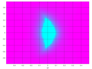
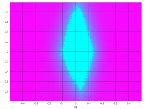
I’ve made a lot of statistical eyes scans for the said USB channel. This mechanism is made by Xilinx’ transceivers themselves, and is described in the respective user guides. In a nutshell, these scans show how the bit error rate is affected by moving the sampling time from the point that the CDR locks on, as well as adding a voltage offset to the detection threshold. The cyan-colored spot in the middle of the plots shows the region of zero bit errors, and hence it size displays the margins in time and voltage for retaining zero BER.
The important part is the margin in time. In the plots below, UI is the time unit used. One UI corresponds to a bit’s period (i.e. the following bit appears at UI = 1). The vertical axis is less well defined and less important, since voltage is meaningless: It can be amplified as needed. The shape of the eye plot can however give a hint sometimes about certain problems.
The plots in this post were all made on a USB 3.0 data stream (running at the standard 5 Gb/s with scrambler applied), created by a Renesas uPD720202 USB controller (PCI ID 1912:0015), received by the FPGA’s transceiver.
The physical connection, except for PCB traces, involved a Type A connector, connected to a Micro B connector with a high-quality 1 meter USB cable. The Micro-B connector is part of an sfp2usb adapter, which physically connects the signal to the SFP+ connector inside an SFP+ cage, which in turn is connected directly to the FPGA. The signal traces of the sfp2usb adapter are about the length of the SFP+ cage.
So overall, it’s the USB controller chip, PCB trace, USB type A connector mating, 1 meter of cable, Micro B connector mating, a short PCB trace on the sfp2usb adapter, an SFP+ connector mating, PCB trace on the FPGA board reaching the FPGA’s transceiver.
The Renesas USB controller was selected over other options because it showed relatively low signal quality compared with other USB signal sources. The differences are more apparent with this source, however the other sources all gave similar results.
Needless to say, testing at a specific rate with specific equipment doesn’t prove anything on the general quality of the transceivers, and yet the 5 Gb/s represents a medium rate channel quite well.
The FPGA boards used:
- Xilinx KCU105 for Kintex Ultrascale
- Xilinx KC705 for Kintex-7
- Trenz TE0714 for Artix-7 with carrier board having an SFP+ cage
I used some home-cooked logic for making the eye scans and Octave to produce the plots, so if the format doesn’t look familiar, that’s why.
LPM vs. DFE with Ultrascale GTH
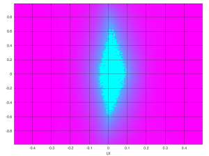
This is the eye scan plot for LPM (click to enlarge the plots):

Eye scan with Ultrascale GTH, LPM equalizer, 5 Gb/s
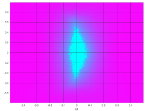
And this is for DFE, with insertion loss set below the 10 dB threshold:

Eye scan with Ultrascale GTH, DFE equalizer, 5 Gb/s, low insertion loss
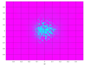
And this is DFE again, with insertion loss set to 14 dB:

Eye scan with Ultrascale GTH, DFE equalizer, 5 Gb/s, 14 dB insertion loss
It’s quite evident that something went horribly wrong when the insertion loss was set to 14 dB, and hence the AGC was enabled, as explained above. But what is even more surprising is that even with the AGC issue away, the eye scan for DFE is slightly worse than LPM. There are three connectors on the signal paths, each making its reflections. DFE should have done better.
Comparing DFE scans with Kintex-7′s GTX
Here’s the proper DFE eye scan for Ultrascale’s GTH again (click to enlarge):

Eye scan with Ultrascale GTH, DFE equalizer, 5 Gb/s, low insertion loss
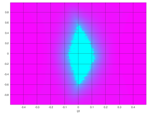
And this is Kintex-7, same channel but with a GTX, having considerably less equalizer taps:

Eye scan with Kintex-7 GTX, DFE equalizer, 5 Gb/s
It’s quite clear that the zero-BER region is considerably larger on the Kintex-7 eye scan. Never mind the y-axis of the plot, it’s the time axis that matters, and it’s clearly wider. Kintex-7 did better than Ultrascale.
Comparing LPM scans with GTX / GTP
This is the LPM eye scan for Ultrascale’s GTH again:

Eye scan with Ultrascale GTH, LPM equalizer, 5 Gb/s
And Kintex-7′s counterpart:

Eye scan with Kintex-7 GTX, LPM equalizer, 5 Gb/s
It’s clearly better than Ultrascale’s scan. Once again, never mind that the zero-BER part looks bigger: Compare the margin in the time axis. Also note that Kintex-7′s DFE did slightly better than LPM, as expected.
And since Artix-7 is also capable of LPM, here’s its scan:

Eye scan with Artix-7 GTP (LPM equalizer), 5 Gb/s
Surprise, surprise: Atrix-7′s eye scan was best of all options. The low-cost, low-power device took first prize. And it did so with an extra connector with the carrier board.
Maybe this was pure luck. Maybe it’s because the scan was obtained with a much smaller board, with possibly less PCB trace congestion. And maybe the LPM on Artix-7 is better because there’s no DFE on this device, so they put an extra effort on LPM.
Conclusion
The main takeaway from this experience of mine is that advanced doesn’t necessarily mean better. Judging by the results, it seems to be the other way around: Ultrascale’s GTH being more fussy about the signal, and losing to Kintex-7′s GTX, and both losing to Artix-7.
And also, to take the insertion loss setting in the Wizard seriously.
As I’ve already said above, this is just a specific case with specific equipment. And yet, the results turned out anything but intuitive.
Appendix: Equalizers, ISI and Nyquist frequency, really briefly
First, the Nyquist frequency: It’s just half the raw bit rate on wire. For example, it’s. 2.5 GHz for a USB Superspeed link with 5 Gb/s raw data rate. The idea behind this term is that the receiver makes one analog sample per bit period, and Nyquist’s Theorem does the rest. But it’s also typically the frequency at which one can low-pass filter the channel without any significant effect.
Next, what’s this insertion loss? For those who haven’t played with RF network analyzers for fun, insertion loss is, for a given frequency, the ratio between the inserted signal power on one side of the cable and/or PCB trace and the power that arrives at the other end. You could call it the frequency-dependent attenuation of the signal. As the frequency rises, this ratio tends to rise (more loss of energy) as this energy turns into radio transmission and heat. Had this power loss been uniform across frequency, it would have been just a plain attenuation, which is simple to correct with an amplifier. The frequency-varying insertion loss results in a distortion of the signal, typically making the originally sharp transitions in time between ’0′ and ’1′ rounder and smeared along possibly several symbol periods.
This smearing effect results in Intersymbol Interference (ISI), which means that when the bit detector samples the analog voltage for determining whether its a ’0′ or ’1′, this analog voltage is composed of a sum of voltages, depending on several bits. These additional voltage components act a bit like noise and increase the bit error rate (BER), however this isn’t really noise (such as the one picked up by crosstalk or created by the electronics), but rather the effect of a bit’s analog signal being spread out over a longer time period.
Another, unrelated reason for ISI is reflections: As the analog signal travels as an electromagnetic wave through the PCB copper trace or cable, reflections are created when the medium changes or makes sharp turns. This could be a via on the PCB board (or just a poorly designed place on the layout), or a connector, which involves several medium transitions: From the copper trace on the PCB to the connector’s leg, from one side of the connector to the connector mating with it, and then from the connector’s leg to the medium that carries the signal further. This assuming the connector doesn’t have any internal irregularities.
So ISI is what equalizers attempt to fix. There’s a relatively simple approach, employed by the linear equalizer. It merely attempts to insert a filter with a frequency response that compensates for the channel’s insertion loss pattern: The equalizer amplifies high frequencies and attenuates low frequencies. By doing so, some of the insertion loss’ effect is canceled out. This reverse filter is tuned by the equalizer for optimal results, and when this works well, the result is an improvement of the ISI. The linear equalizer doesn’t help at all regarding reflections however.
The transmitter can help with this matter by shaping its signal to contain more high-frequency components — this is called pre-emphasis — but that’s a different story.
The DFE (Decision Feedback Equalizer) attempts to fix the ISI directly. It’s designed with the assumption that the transmitted bits in the channel are completely random (which is often ensured by applying a scrambler to the bit stream). Hence the voltages that are sampled by the bit detector should be linearly uncorrelated, and when there is such correlation, it’s attributed to ISI.
This equalizer cancels the correlation between the bit that is currently detected and the analog voltages of a limited number of bits that will be detected after it. This is done by adding or subtracting a certain voltage for each of the signal samples that are used for detecting the bits after the current one. The magnitude of this operation (which can be negative, of course) depends on the time distance between the current bit and the one manipulated. Whether its an addition or subtraction depends on whether the current bit was detected as a ’0′ or ’1′.
The result is hence that when the sample arrives at the bit detector, it’s linearly uncorrelated with the bits that were detected before it. Or more precisely, uncorrelated with a number of bits detected before it, depending on the number of taps that the DFE has.
This method is more power consuming and has a strong adverse effect if the bits aren’t random. It’s however considered better, in particular for canceling the effect of signal reflections, which is a common problem as the analog signal travels on the PCB and/or cable and reaches discontinuities (vias, connectors etc.).
Having said that, one should remember that the analog signal typically travels at about half the speed of light on PCB traces (i.e. 1.5 x 10^8 m/s), so e.g. at 5 Gb/s each symbol period corresponds to 3 cm. Accordingly, an equalizer with e.g. 8 taps is able to cancel reflections that have traveled 24 cm (typically 12 cm in each direction). So DFE may help with reflections on PCBs, but not if the reflection has gone back and forth through a longer cable. Which may not an issue, since the cable itself typically attenuates the reflection’s signal as it goes back and forth.
According to the user guides, when a Xilinx transceiver is set to LPM (Low Power Mode), only a linear equalizer is employed. When DFE is selected, a linear equalizer, followed by a DFE equalizer are employed.
Introduction
Unlike Firefox, Google Chrome doesn’t allow editing passwords (at least not the version I have, and it seems like this feature will be added). One possible workaround is to enable Google Sync for passwords, and have those stored on the server: It’s possible to edit the passwords at passwords.google.com. If you have no problem with Google keeping track of all your passwords, definitely go for it.
Alternatively, export the passwords, edit the CSV file and re-import the relevant password.
To export the passwords, go: Topleft dots button > Settings > Passwords > Topleft dots button > Export passwords…
To import the password, pick Import on the same menu (i.e. the one with Export passwords…). Odds are that you don’t have that option. It needs to be enabled, see below.
The password list is a plain CSV file, so make sure its well protected and preferably deleted soon. I suggest deleting all lines except for the title line and the one containing the password to be changed. No point fiddling with all the others.
Enable password import
This needs to be done once and for all, so Google Chrome has an “Import” option in its password list setting button (see this page). So type chrome://flags on the address bar, search for “Password import” and change it from “Default” to “Enabled”. Chrome will request a relaunch. Go for it.
General
These are my notes as I set up the jitter attenuator devices (Silicon Labs’ Si5324 and Si5328) on Xilinx development boards as clean clock sources for use with MGTs. As such, this post isn’t all that organized.
I suppose that the reason Xilinx put a jitter attenuator to drive the SFP+ related reference clock, rather than just a plain clock generator, is first and foremost because it can be used as a high-quality clock source anyhow. On top of that, it may sync on a reference clock that might be derived from some other source. In particular, this allows syncing the SFP+ module’s data rate with the data rate of an external data stream.
But it’s a bit of a headache to set up. But if you’re into FPGAs, you should be used to this already.
Jots on random topics
- To get the register settings, run DSPLLsim, a tool issued by Silicon Labs (part of Precision Clock EVB Software). There is no need for any evaluation board to run this tool for the sake of obtaining register values, and neither is there any need to install the drivers it suggests to install during the software’s installation.
- Note that there’s an outline for the settings to make with DSPLLsim in a separate section below, which somewhat overlaps these jots.
- Enable Free Run Mode = the crystal, which is connected to XA/XB is routed to CKIN2. So there’s no need to feed the device with a clock, but instead set the reference clock to CKIN2. That works as a 114.285 MHz (± 20 ppm) reference clock on all Xilinx boards I’ve seen so far, including KC705, ZC706, KCU105, ZCU106, KCU116, VC707, VC709, VCU108 and VCU118). This is also the frequency recommended in the Silicon Lab’s docs for a crystal reference.
- The clock outputs should be set to LVDS. This is how they’re treated on Xilinx’ boards.
- f3 is the frequency at the input of the phase detector (i.e. the reference clock after division). The higher f3, the lower jitter.
- The chip’s CMODE is tied to GND, so the interface is I2C.
- RATE0 and RATE1 are set to MM by not connecting them, so the internal pull-up-and-down sets them to this mode. This setting requires a 3rd overtone crystal with a 114.285 MHz frequency, which is exactly what’s in the board (see Si53xx Reference Manual, Appendix A, Table 50).
- The device’s I2C address depends on the A2-A0 pins, which are all tied to GND on the boards I’ve bothered to check. The 7-bit I2C address is { 4b’1101, A[2:0] }. Since A=0, it’s 7-bit address 0x68, or 0xD0 / 0xD1 in 8-bit representation.
- Except for SCL, SDA, INT_C1B and RST_B, there are no control pins connected to the FPGA. Hence all other outputs can be configure to be off. RST_B is an input to reset the device. INT_C1B indicates problems with CKIN1 (only) which is useless in Free Run Mode, or may indicate an interrupt condition, which is more useful (but not really helpful due to the catch explained a few bullets down).
- Hence be INT_PIN and CK1_BAD_PIN (bits 0 and 2 in register 20) should be ’1′, so that INT_C1B functions as an interrupt pin. The polarity of this pin is set by bit 0 of register 22 (INT_POL). Also set LOL_MSK to ’1′ (bit 0 of register 24), so that INT_C1B is asserted until the PLL is locked. This might take several seconds if the loop bandwidth is narrow (which is good for jitter), so the FPGA should monitor this pin and hold the CPLL in reset until the reference clock is stable.
- There is a catch, though: The INT_C1B pin reflects the value of the internal register LOL_FLG (given the outlined register setting), which latches a Loss Of Lock, and resets it only when zero is written to bit 0 of register 132. Or so I understand from the datasheet’s description for register 132, saying “Held version of LOL_INT. [ ... ] Flag cleared by writing 0 to this bit.” Also from Si53xx Reference Manual, section 6.11.9: “Once an interrupt flag bit is set, it will remain high until the register location is written with a ’0′ to clear the flag”. Hence the FPGA must continuously write to this register, or INT_C1B will be asserted forever. This could have been avoided by sensing the LOL output, however it’s not connected to the FPGA.
- Alternatively, one can poll the LOL_INT flag directly, as bit 0 in register 130. If the I2C bus is going to be continuously busy until lock is achieved, one might as well read the non-latched version directly.
- To get an idea of lock times, take a look on Silicon Labs’ AN803, where lock times of minutes are discussed as a normal thing. Also the possibility that lock indicator (LOL) might go on and off while acquiring lock, in particular with old devices.
- Even if the LOL signal wobbles, the output clock’s frequency is already correct, so it’s a matter of slight phase adjustments, made with a narrow bandwidth loop. So the clock is good enough to work with as soon as LOL has gone low for the first time, in particular in a case like mine, where the CPLL should be able to tolerate a SSC running between 0 and -5000 ppm at a 33 kHz rate.
- It gets better: Before accessing any I2C device on the board, the I2C switch (PCA9548A) must be programmed to let the signal through to the jitter attenuator: It wakes up with all paths off. The I2C switch’ own 7-bit address is { 4b’1110, A[2:0] }, where A[2:0] are its address pins. Check the respective board’s user guide for the actual address that has been set up.
- Checking the time to lock on an Si5324 with a the crystal as reference, it went all from 600 ms to 2000 ms. It seems like it depends on the temperature of something, the warmer the longer lock time: Turning off the board for a minute brings back the lower end of lock times. But I’ve also seen quite random lock times, so don’t rely on any figure nor that it’s shorter after powerup. Just check the LOL and be ready to wait.
- As for Si5328, lock times are around 20 seconds (!). Changing the loop bandwidth (with BWSEL) didn’t make any dramatic difference.
- I recommend looking at the last page of Silicon Lab’s guides for the “We make things simple” slogan.
Clock squelch during self calibration
According to the reference manual section 6.2.1, the user must set ICAL = 1 to initiate a self-calibration after writing new PLL settings with the I2C registers. This initiates a self calibration.
To avoid an output clock that is significantly off the desired frequency, SQ_ICAL (bit 4 in register 4) should be set to ’1′, and CKOUT_ALWAYS_ON (bit 5 in register 0) should be ’0′. “SQ_ICAL” stands for squelch the clock until ICAL is completed.
The documentation is vague on whether the clock is squelched until the internal calibration is done, or until the lock is complete (i.e. LOL goes low). The reference manual goes “if SQ_ICAL = 1, the output clocks are disabled during self-calibration and will appear after the self-calibration routine is completed”, so this sounds like it doesn’t wait for LOL to go low. However the truth table for CKOUT_ALWAYS_ON and SQ_ICAL (Table 28 in the reference manual, and it also appears in the data sheets) goes “CKOUT OFF until after the first successful ICAL (i.e., when LOL is low)”. Nice, huh?
And if it there is no clock when LOL is high, what if it wobbles a bit after the initial lock acquisition?
So I checked this up with a scope on an Si5324 locking on XA/XB, with SQ_ICAL=1 and CKOUT_ALWAYS_ON=0, and the output clock was squelched for about 400 μs, and then became active throughout 1.7 seconds of locking, during which LOL was low. So it seems like there’s no risk of the clock going on and off if LOL wobbles.
LOCKT
This parameter controls the lock detector, and wins the prize for the most confusing parameter.
It goes like this: The lock detector monitors the phase difference with the reference clock. If the phase difference looks fine for a certain period of time (determined by the LOCKT parameter), LOL goes low to indicate a successful lock. As a side note, since LOCKT is the time it takes to determine that nothing bad has happened with the phase, it’s the minimum amount of time that LOL will be high, as stated in the reference manual.
But then there’s Table 1 in AN803, showing how LOCKT influences the locking time. Like, really dramatically. From several seconds to a split second. How could a lock detector make such a difference? Note that LOCKT doesn’t have anything to do with the allowed phase difference, but just how long it needs to be fine until the lock detector is happy.
The answer lies in the fast lock mechanism (enabled by FAST_LOCK). It’s a wide bandwidth loop used to make the initial acquisition. When the lock detector indicates a lock, the loop is narrowed for the sake of achieving low jitter. So if the lock detector is too fast, switching to the low bandwidth loop occurs to early, and it will take a longer time to reach a proper lock. If it’s too slow (and hence fussy), it wastes time on the wide bandwidth phase.
In the end, the datasheet recommends a value of 0x1 (53 ms). This seems to be the correct fit-all balance.
Another thing that AN803 mentions briefly, is that LOL is forced high during the acquisition phase. Hence the lock detection, which switches the loop from acquisition (wide loop bandwidth) to low-jitter lock (narrow bandwidth) is invisible to the user, and for a good reason: The lock detector is likely to wobble at this initial stage, and there’s really no lock. The change made in January 2013, which is mentioned in this application note, was partly for producing a LOL signal that would make sense to the user.
DSPLLsim settings
Step by step for getting the register assignments to use with the device.
- After starting DPLLsim, select “Create a new frequency plan with free running mode enabled”
- In the next step, select the desired device (5328 or 5324).
- In the following screen, set CKIN1 to 114.285 MHz and CKOUT1 to the desired output frequency (125 MHz in my case). Also set the XA-XB input to 114.285 MHz. Never mind that we’re not going to work with CKOUT1 — this is just for the sake of calculating the dividers’ values.
- Click “Calculate ratio” and hope for some pretty figures.
- The number of outputs can remain 2.
- Click “Next”.
- Now there’s the minimal f3 to set. 16 kHz is a bit too optimistic. Reducing it to 14 kHz was enough for the 125 MHz case. Click “Next” again.
- Now a list of frequency plans appears. If there are several options, odds are that you want the one with the highest f3. If there’s just one, fine. Go for it: Select that line and click “Next” twice.
- This brings us to the “Other NCn_LS Values” screen, which allows setting the output divisor of the second clock output. For the same clock on both outputs, click “Next”.
- A summary of plan is given. Review and click “OK” to accept it. It will appear on the next window as well.
And this brings us to the complicated part: The actual register settings. This tool is intended to run against an evaluation module, and update its parameters from the computer. So some features won’t work, but that doesn’t matter: It’s the register’s values we’re after.
There are a few tabs:
- “General” tab: The defaults are OK: In particular, enable FASTLOCK, pick the narrowest bandwidth in range with BWSEL. The RATE attribute doesn’t make any difference (it’s set to MM by virtue of pins on the relevant devices). The Digital Hold feature is irrelevant, and so are its parameters (HIST_DEL and HIST_AVG). It’s only useful when the reference clock is shaky.
- “Input Clocks” tab: Here we need changes. Set AUTOSEL_REG to 0 (“Manual”) and CKSEL_REG to 1 for selecting CKIN2 (which is where the crustal is routed to). CLKSEL_PIN set to 0, so that the selection is set by registers and not from any pins. We want to stick to the crystal, no matter what happens on the other clock input. Other than that, leave the defauls: CK_ACTV_POL doesn’t matter, because the pin is unused, and same goes for CS_CA. BYPASS_REG is correctly ’0′ (or the input clock goes directly to output). LOCKT should remain 1 and and VALT isn’t so important in a crystal reference scenario (they set the lock detector’s behavior). The FOS feature isn’t used, so its parameters are irrelevant as well. Automatic clock priority is irrelevant, as manual mode is applied. If you want to be extra pedantic, set CLKINnRATE to 0x3 (“95 to 215 MHz”), which is the expected frequency, at least on CKIN2. And set FOSREFSEL to 0 for XA/XB. It won’t make any difference, as the FOS detector’s output is ignored.
- “Output Clocks” tab: Set the SFOUTn_REG to LVDS (0x7). Keep the defaults on the other settings. In particular, CKOUT_ALWAYS_ON unset and SQ_ICAL set ensures that a clock output is generated only after calibration. No hold logic is desired either.
- “Status” tab: Start with unchecking everything, and set LOSn_EN to 0 (disable). Then check only INT_PIN, CK1_BAD_PIN and LOL_MSK. This is discussed in the jots above. In particular, it’s important that none of the other *_MSK are checked, or the interrupt pin will be contaminated by other alarms. Or it’s unimportant, if you’re going to ignore this pin altogether, and poll LOL through the I2C interface.
The other two tabs (“Register Map” and “Pin Out”) are just for information. No settings there.
So now, the finale: Write the settings to a file. On the main menu go to Options > Save Register Map File… and, well. For extra confusion, the addresses are written in decimal, but the values in hex.
The somewhat surprising result is that the register setting for Si5324 and Si5328 are identical, even though the loop bandwidth is dramatically different: Even though both have BWSEL_REG set to 0x3, which is the narrowest bandwidth possible for either device, for Si5324 it means 8 Hz, and for Si5328 it’s 0.086 Hz. So completely different jitter performance as well as lock time (much slower on Si5328) are expected despite, once again, exactly the same register setting.
There is a slight mistake in the register map: There is no need to write to the register at address 131, as it contains statuses. And if anything, write zeroes to bits [2:0], so that these flags are maybe cleared, and surely not ones. The value in the register map is just the default value.
Same goes for register 132, but it’s actually useful to write to it for the sake of clearing LOL_FLG. Only the value in the register map is 0x02, which doesn’t clear this flag (and once again, it’s simply the default).
It’s worth to note that the last assignment in the register map is writing 0x40 to address 136, which initiates self calibration.
I2C interface
Silicon Lab’s documentation on the I2C interface is rather minimal (see Si53xx Reference Manual, section 6.13), and refers to the standard for the specifics (with a dead link). However quite obviously, the devices work with the common setting for register access with a single byte address: First byte is the I2C address, second is the register address, and the third is the data to be written. All acknowledged.
For a read access, it’s also the common method of a two-byte write sequence to set the register address, a restart (no stop condition) and one byte for the I2C address, and the second reads data.
If there’s more than one byte of data, the address is auto-incremented, pretty much as usual.
According to the data sheet, the RST pin must be asserted (held low) at least 1 μs, after which the I2C interface can be used no sooner than 10 ms (tREADY in the datasheets). It’s also possible to use the I2C interface to induce a reset with the RST_REG bit of register 136. The device performs a power-up reset after powering up (section 5.10 in the manual) however resetting is a good idea to clear previous register settings.
As for the I2C mux, there are two devices used in Xilinx’ boards: TCA9548A and PCA9548A, which are functionally equivalent but with different voltage ranges, according to TI: “Same functionality and pinout but is not an equivalent to the compared device”.
The I2C interface of the I2C mux consists of a single register. Hence there is no address byte. It’s just the address of the device followed by the setting of the register. Two bytes, old school style. Bit n corresponds to channel n. Setting a bit to ’1′ enables the channel, and setting it to ’0′ disconnects it. Plain and simple.
The I2C mux has a reset pin which must be high during operation. On KCU105, it’s connected to the FPGA with a pull-up resistor, so it’s not clear why UG917 says it “must be driven High”, but it clearly mustn’t be driven low. Also on KCU105, the I2C bus is shared between the FPGA and a “System Controller”, which is a small Zynq device with some secret sauce software on it. So there are two masters on a single I2C bus by plain wiring.
According to UG917′s Appendix C, the system controller does some initialization on power-up, hence generating traffic on the I2C bus. Even though it’s not said explicitly, it’s plausible to assume that it’s engineered to finish its business before the FPGA has had a chance to load its bitstream and try its own stunts. Unless the user requests some operations via the UART interface with the controller, but that’s a different story.
… or why does my GTH/GTY not come out of reset? Why are those reset_rx_done / reset_tx_done never asserted after a reset_all or a reset involving the CPLLs?
What’s this CPLL calibration thing about?
It turns out that some GTH/GTY’s on Ultrascale and Ultrascale+ FPGAs have problems with getting the CPLL to work reliably. I’ll leave PG182 for the details on which ones. So CPLL calibration is a cute name for some workaround logic, based upon the well-known principle, that if something doesn’t work, turn it off, turn it on, and then check again. Repeat.
Well, not quite that simple. There’s also some playing with a bit (they call it FBOOST, jump start or not?) in the secret-sauce CPLL_CFG0 setting.
This way or another, this extra piece of logic simply checks whether the CPLL is at its correct frequency, and if so, it does nothing. If the CPLL’s frequency isn’t as expected, with a certain tolerance, it powers the CPLL off and on (with CPLLPD), resets it (CPLLRESET) and also plays with that magic FBOOST bit. And then tries again, up to 15 times.
The need for access to the GT’s DRPs is not just for that magic register’s sake, though. One can’t just measure the CPLL’s frequency directly, as it’s a few GHz. An FPGA can only work with a divided version of this clock. As there are several possibilities for routing and division of clocks inside the GT to its clock outputs, and the clock dividers depend on the application’s configuration, there’s a need to bring one such clock output to give the CPLL’s output divided by a known number. TXOUTCLK was chosen for this purpose.
So much of the calibration logic does exactly that: It sets some DRP registers to set up a certain relation between the CPLL’s output and TXOUTCLK (divided by 20, in fact), it does its thing, and then returns those register’s values to what they were before.
A word of warning
My initial take on this CPLL calibration thing was to enable it for all targets (see below for how). Can’t hurt, can it? An extra check that the CPLL is fine before kicking off. What could possibly go wrong?
I did this on Vivado 2015.2, and all was fine. And then I tried on later Vivado version. Boom. The GTH didn’t come out of reset. More precisely, the CPLL calibration clearly failed.
I can’t say that I know exactly why, but I caught the change that makes the difference: Somewhere between 2015.2 and 2018.3, the Wizard started to set the GTH’s CPLL_INIT_CFG0 instantiation parameter to 16′b0000001010110010. Generating the IP with this parameter set to its old value, 16′b0000000000011110, made the GTH work properly again.
I compared the reset logic as well as the CPLL calibration logic, and even though there I found a few changes, they were pretty minor (and I also tried to revert some of them, but that didn’t make any difference).
So the conclusion is that the change in CPLL_INIT_CFG0 failed the CPLL calibration. Why? I have no idea. The meaning of this parameter is unknown. And the CPLL calibration just checks that the frequency is OK. So maybe it slows down the lock, so the CPLL isn’t ready when it’s checked? Possibly, but this info wouldn’t help very much anyhow.
Now, CPLL calibration is supposed to be enabled only for FPGA targets that are known to need it. The question is whether the Transceiver IP’s Wizard is clever enough to set CPLL_INIT_CFG0 to a value that won’t make the calibration fail on those. I have no idea.
By enabling CPLL calibration for a target that doesn’t need it, I selected an exotic option, but the result should have worked nevertheless. Surely it shouldn’t break from one Vivado version to another.
So the bottom line is: Don’t fiddle with this option, and if your GTH/GTY doesn’t come out of reset, consider turning CPLL calibration off, and see if that changes anything. And if so, I have no clear advice what to do. But at least the mystery will be resolved.
Note that…
- The CPLL calibration is triggered by the GT’s reset_all assertion, as well as with reset_*_pll_and_datapath, if the CPLL is used in the relevant data path. The “reset done” signal for a data path that depends on the CPLL is asserted only if and when the CPLL calibration was successful and the CPLL is locked.
- If cplllock_out (if exposed) is never asserted, this could indicate that the CPLL calibration failed. So it makes sense to wait indefinitely for it — better fail loudly than work with a wobbling clock.
- Because the DRP clock is used to measure the period of time for counting the number of cycles of the divided CPLL clock, its frequency must be set accurately in the Wizard. Otherwise, the CPLL calibration will most certainly fail, even if the CPLL is perfectly fine.
- The calibration state machine takes control of some GT ports (listed below) from when cpllreset_in is deasserted, and until the calibration state machine has finished, with success or failure.
- While the calibration takes place, and if the calibration ends up failing, the cplllock_out signal presented to the user logic is held low. Only when the calibration is finished successfully, is the GT’s CPLLLOCK connected to the user logic (after a slight delay, and synchronized with the DRP clock).
Activating the CPLL calibration feature
See “A word of warning” above. You probably don’t want to activate this feature for all FPGA targets.
There are three possible choices for whether the CPLL calibration module is activated in the Wizard’s transceiver. This can’t be set from the GUI, but by editing the XCI file manually. There are two parameters in that file, PARAM_VALUE.INCLUDE_CPLL_CAL and MODELPARAM_VALUE.C_INCLUDE_CPLL_CAL, which should have the same value as follows:
- 0 — Don’t activate.
- 1 — Do activate.
- 2 — Activate only for devices which the Wizard deems have a problem (default).
Changing it from the default 2 to 1 makes Vivado respond with locking the core saying it “contains stale content”. To resolve this, “upgrade” the IP, which triggers a warning that user intervention is necessary.
And indeed, three new ports are added, and this change this addition of ports is also reflected in the XCI file (but nothing else should change): gtwiz_gthe3_cpll_cal_txoutclk_period_in, gtwiz_gthe3_cpll_cal_cnt_tol_in and gtwiz_gthe3_cpll_cal_bufg_ce_in.
These are three input ports, so they have to be assigned values. PG182‘s Table 3-1 gives the formulas for that (good luck with that) and the dissection notes below explain these formulas. But the TL;DR version is:
- gtwiz_gthe3_cpll_cal_bufg_ce_in should be assigned with a constant 1′b1.
- gtwiz_gthe3_cpll_cal_txoutclk_period_in should be assigned with the constant value of P_CPLL_CAL_TXOUTCLK_PERIOD, as found in the transceiver IP’s synthesis report (e.g. mytransceiver_synth_1/runme.log).
- gtwiz_gthe3_cpll_cal_cnt_tol_in should be assigned with the constant value of P_CPLL_CAL_TXOUTCLK_PERIOD, divided by 100.
The description here relates to a single transceiver in the IP.
The meaning of gtwiz_gthe3_cpll_cal_txoutclk_period_in is as follows: Take the CPLL clock and divide it by 80. Count the number of clock cycles in a time period corresponding to 16000 DRP clock cycles. That’s the value to assign, as this is what the CPLL calibration logic expects to get.
gtwiz_gthe3_cpll_cal_cnt_tol_in is the number of counts that the result can be higher or lower than expected, and still the CPLL will be considered fine. As this is taken as the number of expected counts, divided by 100, this results in a ±1% clock frequency tolerance. Which is a good idea, given that common SSC clocking (PCIe, SATA, USB 3.0) might drag down the clock frequency by -5000 ppm, i.e. -0.5%.
The possibly tricky thing with setting these correctly is that they depend directly on the CPLL frequency. Given the data rate, there might be more than one possibility for a CPLL frequency, however it’s not expected that the Wizard will change it from run to run unless something fundamental is changed in the parameters (e.g. changing the data rate of one of the directions or both).
Besides, the CPLL frequency appears in the XCI file as MODELPARAM_VALUE.C_CPLL_VCO_FREQUENCY.
If the CPLL is activated deliberately, it’s recommended to verify that it actually takes place by setting a wrong value for gtwiz_gthe3_cpll_cal_txoutclk_period_in, and check that the calibration fails (cplllock_out remains low).
Which ports are affected?
Looking at ultragth_gtwizard_gthe3.v gives the list of ports that the CPLL calibration logic fiddles with. Within the CPLL calibration generate clause they’re assigned with certain values, and in the “else” clause, with the plain bypass:
    // Assign signals as appropriate to bypass the CPLL calibration block when it is not instantiated
    else begin : gen_no_cpll_cal
      assign txprgdivresetdone_out = txprgdivresetdone_int;
      assign cplllock_int          = cplllock_ch_int;
      assign drprdy_out            = drprdy_int;
      assign drpdo_out             = drpdo_int;
      assign cpllreset_ch_int      = cpllreset_int;
      assign cpllpd_ch_int         = cpllpd_int;
      assign txprogdivreset_ch_int = txprogdivreset_int;
      assign txoutclksel_ch_int    = txoutclksel_int;
      assign drpaddr_ch_int        = drpaddr_int;
      assign drpdi_ch_int          = drpdi_int;
      assign drpen_ch_int          = drpen_int;
      assign drpwe_ch_int          = drpwe_int;
    end
Dissection of Wizard’s output
The name of the IP was ultragth in my case. That’s the significance of this name appearing all over this part.
The impact of changing the XCI file: In the Verilog files that are produced by the Wizard, MODELPARAM_VALUE.C_INCLUDE_CPLL_CAL is used directly when instantiating the ultragth_gtwizard_top, as the C_INCLUDE_CPLL_CAL instantiation parameter.
Also, the three new input ports are passed on to ultragth_gtwizard_top.v, rather than getting all zero assignments when they’re not exposed to the user application logic.
When activating the CPLL calibration (setting INCLUDE_CPLL_CAL to 1) additional constraints are also added to the constraint file for the IP, adding a few new false paths as well as making sure that the timing calculations for the TXOUTCLK is set according to the requested clock source. The latter is necessary, because the calibration logic fiddles with TXOUTCLKSEL during the calibration phase.
In ultragth_gtwizard_top.v the instantiation parameters and the three ports are just passed on to ultragth_gtwizard_gthe3.v, where the action happens.
First, the following defines are made (they like short names in Xilinx):
`define ultragth_gtwizard_gthe3_INCLUDE_CPLL_CAL__EXCLUDE 0
`define ultragth_gtwizard_gthe3_INCLUDE_CPLL_CAL__INCLUDE 1
`define ultragth_gtwizard_gthe3_INCLUDE_CPLL_CAL__DEPENDENT 2
and further down, we have this short and concise condition for enabling CPLL calibration:
    if ((C_INCLUDE_CPLL_CAL         == `ultragth_gtwizard_gthe3_INCLUDE_CPLL_CAL__INCLUDE) ||
        (((C_INCLUDE_CPLL_CAL       == `ultragth_gtwizard_gthe3_INCLUDE_CPLL_CAL__DEPENDENT) &&
         ((C_GT_REV                 == 11) ||
          (C_GT_REV                 == 12) ||
          (C_GT_REV                 == 14))) &&
         (((C_TX_ENABLE             == `ultragth_gtwizard_gthe3_TX_ENABLE__ENABLED) &&
           (C_TX_PLL_TYPE           == `ultragth_gtwizard_gthe3_TX_PLL_TYPE__CPLL)) ||
          ((C_RX_ENABLE             == `ultragth_gtwizard_gthe3_RX_ENABLE__ENABLED) &&
           (C_RX_PLL_TYPE           == `ultragth_gtwizard_gthe3_RX_PLL_TYPE__CPLL)) ||
          ((C_TXPROGDIV_FREQ_ENABLE == `ultragth_gtwizard_gthe3_TXPROGDIV_FREQ_ENABLE__ENABLED) &&
           (C_TXPROGDIV_FREQ_SOURCE == `ultragth_gtwizard_gthe3_TXPROGDIV_FREQ_SOURCE__CPLL))))) begin : gen_cpll_cal
which simply means that the CPLL calibration module should be generated if _INCLUDE_CPLL_CAL is 1 (as I changed it to), or if it’s 2 (default) and some conditions for enabling it automatically are met).
Further down, the hint for how to assign those three new ports is given. Namely, if CPLL was added automatically due to the default assignment and specific target FPGA, the values calculated by the Wizard itself are used
      // The TXOUTCLK_PERIOD_IN and CNT_TOL_IN ports are normally driven by an internally-calculated value. When INCLUDE_CPLL_CAL is 1,
      // they are driven as inputs for PLL-switching and rate change special cases, and the BUFG_GT CE input is provided by the user.
      wire [(`ultragth_gtwizard_gthe3_N_CH* 18)-1:0] cpll_cal_txoutclk_period_int;
      wire [(`ultragth_gtwizard_gthe3_N_CH* 18)-1:0] cpll_cal_cnt_tol_int;
      wire [(`ultragth_gtwizard_gthe3_N_CH*  1)-1:0] cpll_cal_bufg_ce_int;
      if (C_INCLUDE_CPLL_CAL == `ultragth_gtwizard_gthe3_INCLUDE_CPLL_CAL__INCLUDE) begin : gen_txoutclk_pd_input
        assign cpll_cal_txoutclk_period_int = {`ultragth_gtwizard_gthe3_N_CH{gtwiz_gthe3_cpll_cal_txoutclk_period_in}};
        assign cpll_cal_cnt_tol_int         = {`ultragth_gtwizard_gthe3_N_CH{gtwiz_gthe3_cpll_cal_cnt_tol_in}};
        assign cpll_cal_bufg_ce_int         = {`ultragth_gtwizard_gthe3_N_CH{gtwiz_gthe3_cpll_cal_bufg_ce_in}};
      end
      else begin : gen_txoutclk_pd_internal
        assign cpll_cal_txoutclk_period_int = {`ultragth_gtwizard_gthe3_N_CH{p_cpll_cal_txoutclk_period_int}};
        assign cpll_cal_cnt_tol_int         = {`ultragth_gtwizard_gthe3_N_CH{p_cpll_cal_txoutclk_period_div100_int}};
        assign cpll_cal_bufg_ce_int         = {`ultragth_gtwizard_gthe3_N_CH{1'b1}};
      end
These `ultragth_gtwizard_gthe3_N_CH things are just duplication of the same vector, in case there are multiple channels for the same IP.
First, note that cpll_cal_bufg_ce is assigned constant 1. Not clear why this port is exposed at all.
And now to the calculated values. Given that it says
      wire [15:0] p_cpll_cal_freq_count_window_int      = P_CPLL_CAL_FREQ_COUNT_WINDOW;
      wire [17:0] p_cpll_cal_txoutclk_period_int        = P_CPLL_CAL_TXOUTCLK_PERIOD;
      wire [15:0] p_cpll_cal_wait_deassert_cpllpd_int   = P_CPLL_CAL_WAIT_DEASSERT_CPLLPD;
      wire [17:0] p_cpll_cal_txoutclk_period_div100_int = P_CPLL_CAL_TXOUTCLK_PERIOD_DIV100;
a few rows above, and
  localparam [15:0] P_CPLL_CAL_FREQ_COUNT_WINDOW      = 16'd16000;
  localparam [17:0] P_CPLL_CAL_TXOUTCLK_PERIOD        = (C_CPLL_VCO_FREQUENCY/20) * (P_CPLL_CAL_FREQ_COUNT_WINDOW/(4*C_FREERUN_FREQUENCY));
  localparam [15:0] P_CPLL_CAL_WAIT_DEASSERT_CPLLPD   = 16'd256;
  localparam [17:0] P_CPLL_CAL_TXOUTCLK_PERIOD_DIV100 = (C_CPLL_VCO_FREQUENCY/20) * (P_CPLL_CAL_FREQ_COUNT_WINDOW/(400*C_FREERUN_FREQUENCY));
  localparam [25:0] P_CDR_TIMEOUT_FREERUN_CYC         = (37000 * C_FREERUN_FREQUENCY) / C_RX_LINE_RATE;
it’s not all that difficult to do the math. And looking at Table 3-1 of PG182, the formulas match perfectly, but I didn’t feel very reassured by those.
So why bother? Much easier to use the values calculated by the tools, as they appear in ultragth_synth_1/runme.log (for a 5 Gb/s rate and reference clock of 125 MHz, but YMMV as there’s more than one way to achieve a line rate):
	Parameter P_CPLL_CAL_FREQ_COUNT_WINDOW bound to: 16'b0011111010000000
	Parameter P_CPLL_CAL_TXOUTCLK_PERIOD bound to: 18'b000000111110100000
	Parameter P_CPLL_CAL_WAIT_DEASSERT_CPLLPD bound to: 16'b0000000100000000
	Parameter P_CPLL_CAL_TXOUTCLK_PERIOD_DIV100 bound to: 18'b000000000000101000
	Parameter P_CDR_TIMEOUT_FREERUN_CYC bound to: 26'b00000011100001110101001000
The bottom line is hence to set gtwiz_gthe3_cpll_cal_txoutclk_period_in to 18′b000000111110100000, and gtwiz_gthe3_cpll_cal_cnt_tol_in to 18′b000000000000101000. Which is 4000 and 40 in plain decimal, respectively.
Dissection of CPLL Calibration module (specifically)
The CPLL calibrator is implemented in gtwizard_ultrascale_v1_5/hdl/verilog/gtwizard_ultrascale_v1_5_gthe3_cpll_cal.v.
Some basic reverse engineering. This may be inaccurate, as I wasn’t very careful about the gory details on this matter. Also, when I say that a register is modified below, it’s to values that are listed after the outline of the state machine (further below).
So just to get an idea:
- TXCLKOUTSEL start with value 0.
- Using the DRP ports, it fetches the existing values of the PROGCLK_SEL and PROGDIV registers, and modifies their values.
- It changes TXCLKOUTSEL to 3′b101, i.e. TXCLKOUT is routed to TXPROGDIVCLK. This can be more than one clock source, but it’s the CPLL directly, divided by PROGDIV (judging by the value assigned to PROGCLK_SEL).
- CPLLRESET is asserted for 32 clock cycles, and then deasserted.
The state machine now enters a loop as follows.
- The state machine waits 16384 clock cycles. This is essentially waiting for the CPLL to lock, however the CPLL’s lock detector isn’t monitored. Rather, it waits this fixed amount of time.
- txprogdivreset is asserted for 32 clock cycles.
- The state machine waits for the assertion of the GT’s txprgdivresetdone (possibly indefinitely).
- The state machine checks that the frequency counter’s output (more on this below) is in the range of TXOUTCLK_PERIOD_IN ± CNT_TOL_IN. If so, it exits this loop (think C “break” here), with the intention of declaring success. If not, and this is the 15th failed attempt, it exits the loop as well, but with the intention of declaring failure. Otherwise, it continues as follows.
- The FBOOST DRP register is read and then modified.
- 32 clock cycles later, CPLLRESET is asserted.
- 32 clock cycles later, CPLLPD is asserted for a number of clock cycles (determined by the module’s WAIT_DEASSERT_CPLLPD_IN input), and then deasserted (the CPLL is powered down and up!).
- 32 clock cycles later, CPLLRESET is deasserted.
- The FBOOST DRP register is restored to its original value.
- The state machine continues at the beginning of this loop.
And the final sequence, after exiting the loop:
- PROGDIV and PROGCLK_SEL are restored to its original value
- CPLLRESET is asserted for 32 clock cycles, and then deasserted.
- The state machine waits for the assertion of the GT’s cplllock, possibly indefinitely.
- txprogdivreset is asserted for 32 clock cycles.
- The state machine waits for the assertion of the GT’s txprgdivresetdone (possibly indefinitely).
- The state machine finishes. At this point one of the module’s CPLL_CAL_FAIL or CPLL_CAL_DONE is asserted, depending on the reason for exiting the loop.
As for the values assigned when I said “modified” above, I won’t get into that in detail, but just put a related snippet of code. Note that these values are often shifted to their correct place in the DRP registers in order to fulfill their purpose:
  localparam [1:0]  MOD_PROGCLK_SEL = 2'b10;
  localparam [15:0] MOD_PROGDIV_CFG = 16'hA1A2; //divider 20
  localparam [2:0]  MOD_TXOUTCLK_SEL = 3'b101;
  localparam        MOD_FBOOST = 1'b1;
Now, a word about the frequency counter: It’s a bit complicated because of clock domain issues, but what it does is to divide the clock under test by 4, and then count how many cycles the divided clock has during a period of FREQ_COUNT_WINDOW_IN DRP clocks. Which is hardcoded as 16000 clocks.
If we’ll trust the comment saying that PROGDIV is set to 20, it means that the frequency counter gets the CPLL clock divided by 20. It then divides this further by 4, and counts this for 16000 DRP clocks. Which is exactly the formula given in Table 3-1 of PG182.
Are we having fun?
… or any other “unsupported” Linux distribution.
… or: How to trick the installer into thinking you’re running one of the supported OSes.
So I wanted to install Vivado 2020.1 on my Linux Mint 19 (Tara) machine. I downloaded the full package, and ran xsetup. A splash window appeared, and soon after it another window popped up, saying that my distribution wasn’t supported, listing those that were, and telling me that I could click “OK” to continue nevertheless. Which I did.
But then nothing happened. Completely stuck. And there was an error message on the console, reading:
$ ./xsetup
Exception in thread "SPLASH_LOAD_MESSAGE" java.lang.IllegalStateException: no splash screen available
	at java.desktop/java.awt.SplashScreen.checkVisible(Unknown Source)
	at java.desktop/java.awt.SplashScreen.getBounds(Unknown Source)
	at java.desktop/java.awt.SplashScreen.getSize(Unknown Source)
	at com.xilinx.installer.gui.H.run(Unknown Source)
Exception in thread "main" java.lang.IllegalStateException: no splash screen available
	at java.desktop/java.awt.SplashScreen.checkVisible(Unknown Source)
	at java.desktop/java.awt.SplashScreen.close(Unknown Source)
	at com.xilinx.installer.gui.G.b(Unknown Source)
	at com.xilinx.installer.gui.InstallerGUI.G(Unknown Source)
	at com.xilinx.installer.gui.InstallerGUI.e(Unknown Source)
	at com.xilinx.installer.api.InstallerLauncher.main(Unknown Source)
This issue is discussed in this thread of Xilinx’ forum. Don’t let the “Solved” title mislead you: They didn’t solve it at all. But one of the answers there gave me the direction: Fool the installer to think my OS is supported, after all. In this specific case there was no problem with the OS, but a bug in the installer that caused it to behave silly after that popup window.
It was also suggested to install Vivado in batch mode with
./xsetup -b ConfigGen
however this doesn’t allow for selecting what devices I want to support. And this is a matter of tons of disk space.
So to make it work, I made changes in some files in /etc, and kept the original files in a separate directory. I also needed to move /etc/lsb-release into that directory as well, so it won’t mess up things
I changed /etc/os-release (which is in fact a symlink to ../usr/lib/os-release on my machine, so watch it) to
NAME="Ubuntu"
VERSION="16.04.6 LTS (Xenial Xerus)"
ID=ubuntu
ID_LIKE=debian
PRETTY_NAME="Ubuntu 16.04.6 LTS"
VERSION_ID="16.04"
HOME_URL="http://www.ubuntu.com/"
SUPPORT_URL="http://help.ubuntu.com/"
BUG_REPORT_URL="http://bugs.launchpad.net/ubuntu/"
VERSION_CODENAME=xenial
UBUNTU_CODENAME=xenial
and /etc/lsb-release
DISTRIB_ID=Ubuntu
DISTRIB_RELEASE=16.04
DISTRIB_CODENAME=xenial
DISTRIB_DESCRIPTION="Ubuntu 16.04.6 LTS"
This might very well be an overkill, but once I got the installation running, I didn’t bother check what the minimal change is. Those who are successful might comment below on this, maybe?
Note that this might not work on a Red Hat based OS, because it seems that there are distribution-dependent issues. Since Linux Mint 19 is derived from Ubuntu 18.04, faking an earlier Ubuntu distro didn’t cause any problems.
This failed for me repeatedly at first, because I kept a copy of the original files in the /etc directory. This made the installation tool read the original files as well as the modified ones. Using strace, I found that the tool called cat with
execve("/bin/cat", ["cat", "/etc/lsb-release", "/etc/os-release", "/etc/real-upstream-release"], 0x5559689a47b0 /* 55 vars */) = 0
It looks like “cat” was called with some wildcard, maybe /etc/*-release? So the solution was to move the original files away to a new directory /etc/real/, and create the fake ones in their place.
Another problem was probably that /etc/lsb-release is a directory in my system. That made the “cat” return a failure status, which can’t be good.
Of course I have an opinion on the entire OS support situation, but if you’re reading this, odds that you agree with me anyhow.
Just a quick note to remind myself: There’s a gap between the size of a disk, the used space and the available space. It’s quite well-known that a certain percentage of the disk (that’s 200 GB on a 3.6 TB backup disk) is saved for root-only writes.
So the reminder is: No problem filling the disk beyond the Available = zero blocks point if you’re root. And it doesn’t matter if the files written don’t belong to root. The show goes on.
Also, the numbers shown by df are updated only when the file written to is closed. So if a very long file is being copied, it might freeze for a while, and then boom.
This is important in particular when using the disk just for backing up data, because the process doing the backup is root, but the files aren’t.
But whatever you do, don’t press CTRL-C while the extracting goes on. If tar quits in the middle, there will be file ownerships and permissions unset, and symlinks set to zero-length files too. It wrecks the entire backup, even in places far away from where tar was working when it was stopped.
When to do this
Because Gnome desktop is sure it knows what’s best for me, and it’s virtually impossible to just tell it that I want this screen resolution mode and no other, there is only one option left: Lie about the monitor’s graphics mode capabilities. Make the kernel feed it with fake screen information (EDID), that basically says “there is only this resolution”. Leave it with one choice only.
What is EDID? It’s a tiny chunk of information that is stored on a small EEPROM memory on the monitor. The graphics card fetches this blob through two I2C wires on the cable, and deduces from it what graphics mode (with painfully detailed timing parameters) the monitor supports. It’s that little hex blob that appears when you go xrandr –verbose.
I should mention a post in Gentoo forum, which suggests making X ignore EDID info by using
Option       "UseEDID" "false"
Option       "UseEDIDFreqs" "false"
in /etc/X11/xorg.conf, or is it a file in /usr/share/X11/xorg.conf.d/? And then just set the screen mode old-school. Didn’t bother to check this. There are too many players in this game. Faking EDID seemed to be a much better idea than to ask politely not to consider it.
How to feed a fake EDID
The name of the game is Kernel Mode Setting (KMS). Among others, it allows loading a file from /lib/firmware which is used as the screen information (EDID) instead of getting it from the screen.
For this to work, the CONFIG_DRM_LOAD_EDID_FIRMWARE kernel compilation must be enabled (set to “y”).
Note that unless Early KMS is required, the firmware file is loaded after the initramfs stage. In other words, it’s not necessary to push the fake EDID file into the initramfs, but it’s OK to have it present only in the filesystem that is mounted after the initramfs.
The EDID file should be stored in /lib/firmware/edid (create the directory if necessary) and the following command should be added to the kernel command line:
drm_kms_helper.edid_firmware=edid/fake_edid.bin
(for kernels 4.15 and later, there’s a drm.edid_firmware parameter that is supposed to be better in some way).
Generating a custom EDID file
I needed a special graphics mode to solve a problem with my OLED screen. Meaning I had to cook my own EDID file. It turned out quite easy, actually.
The kernel’s doc for this is Documentation/admin-guide/edid.rst
In the kernel’s tools/edid, edit one of the asm files (e.g. 1920x1080.S) and set the parameters to the correct mode. This file has just defines. The actual data format is produced in edid.S, which is included at the bottom. The output in this case is 1920x1080.bin. Note that the C file (1920x1080.c) is an output as well in this case — for reference of some other use, I guess.
And then just type “make” in tools/edid/ (don’t compile the kernel, that’s really not necessary for this).
The numbers in the asm file are in a slightly different notation, as explained in the kernel doc. Not a big deal to figure out.
In my case, I translated this xrandr mode line
  oledblack (0x10b) 173.000MHz -HSync +VSync
        h: width  1920 start 2048 end 2248 total 2576 skew    0 clock  67.16KHz
        v: height 1080 start 1083 end 1088 total 1120           clock  59.96Hz
to this:
/* EDID */
#define VERSION 1
#define REVISION 3

/* Display */
#define CLOCK 173000 /* kHz */
#define XPIX 1920
#define YPIX 1080
#define XY_RATIO XY_RATIO_16_9
#define XBLANK 656
#define YBLANK 40
#define XOFFSET 128
#define XPULSE 200
#define YOFFSET 3
#define YPULSE 5
#define DPI 96
#define VFREQ 60 /* Hz */
#define TIMING_NAME "Linux FHD"
/* No ESTABLISHED_TIMINGx_BITS */
#define HSYNC_POL 0
#define VSYNC_POL 0

#include "edid.S"
There seems to be a distinction between standard resolution modes and those that aren’t. I got away with this, because 1920x1080 is a standard mode. It may be slightly trickier with a non-standard mode.
When it works
This is what it looks like when all is well. First, the kernel logs. In my case, because I didn’t put the file in the initramfs, loading it fails twice:
[    3.517734] platform HDMI-A-3: Direct firmware load for edid/1920x1080.bin failed with error -2
[    3.517800] [drm:drm_load_edid_firmware [drm_kms_helper]] *ERROR* Requesting EDID firmware "edid/1920x1080.bin" failed (err=-2)
and again:
[    4.104528] platform HDMI-A-3: Direct firmware load for edid/1920x1080.bin failed with error -2
[    4.104580] [drm:drm_load_edid_firmware [drm_kms_helper]] *ERROR* Requesting EDID firmware "edid/1920x1080.bin" failed (err=-2)
But then, much later, it loads properly:
[   19.864966] [drm] Got external EDID base block and 0 extensions from "edid/1920x1080.bin" for connector "HDMI-A-3"
[   93.298915] [drm] Got external EDID base block and 0 extensions from "edid/1920x1080.bin" for connector "HDMI-A-3"
[  109.573124] [drm] Got external EDID base block and 0 extensions from "edid/1920x1080.bin" for connector "HDMI-A-3"
[ 1247.290084] [drm] Got external EDID base block and 0 extensions from "edid/1920x1080.bin" for connector "HDMI-A-3"
Why several times? Well, the screen resolution is probably set up several times as the system goes up. There’s clearly a quick screen flash a few seconds after the desktop goes up. I don’t know exactly why, and at this stage I don’t care. The screen is at the only mode allowed, and that’s it.
And now to how xrandr sees the situation:
$ xrandr -d :0 --verbose
[ ... ]
HDMI3 connected primary 1920x1080+0+0 (0x10c) normal (normal left inverted right x axis y axis) 500mm x 281mm
 Identifier: 0x48
 Timestamp:  21339
 Subpixel:   unknown
 Gamma:      1.0:1.0:1.0
 Brightness: 1.0
 Clones:
 CRTC:       0
 CRTCs:      0
 Transform:  1.000000 0.000000 0.000000
 0.000000 1.000000 0.000000
 0.000000 0.000000 1.000000
 filter:
 EDID:
 00ffffffffffff0031d8000000000000
 051601036d321c78ea5ec0a4594a9825
 205054000000d1c00101010101010101
 010101010101944380907238284080c8
 3500f41911000018000000ff004c696e
 75782023300a20202020000000fd003b
 3d424412000a202020202020000000fc
 004c696e7578204648440a2020200045
 aspect ratio: Automatic
 supported: Automatic, 4:3, 16:9
 Broadcast RGB: Automatic
 supported: Automatic, Full, Limited 16:235
 audio: auto
 supported: force-dvi, off, auto, on
 1920x1080 (0x10c) 173.000MHz -HSync -VSync *current +preferred
 h: width  1920 start 2048 end 2248 total 2576 skew    0 clock  67.16KHz
 v: height 1080 start 1083 end 1088 total 1120           clock  59.96Hz
Compare the EDID part with 1920x1080.c, which was created along with the binary:
{
 0x00, 0xff, 0xff, 0xff, 0xff, 0xff, 0xff, 0x00,
 0x31, 0xd8, 0x00, 0x00, 0x00, 0x00, 0x00, 0x00,
 0x05, 0x16, 0x01, 0x03, 0x6d, 0x32, 0x1c, 0x78,
 0xea, 0x5e, 0xc0, 0xa4, 0x59, 0x4a, 0x98, 0x25,
 0x20, 0x50, 0x54, 0x00, 0x00, 0x00, 0xd1, 0xc0,
 0x01, 0x01, 0x01, 0x01, 0x01, 0x01, 0x01, 0x01,
 0x01, 0x01, 0x01, 0x01, 0x01, 0x01, 0x94, 0x43,
 0x80, 0x90, 0x72, 0x38, 0x28, 0x40, 0x80, 0xc8,
 0x35, 0x00, 0xf4, 0x19, 0x11, 0x00, 0x00, 0x18,
 0x00, 0x00, 0x00, 0xff, 0x00, 0x4c, 0x69, 0x6e,
 0x75, 0x78, 0x20, 0x23, 0x30, 0x0a, 0x20, 0x20,
 0x20, 0x20, 0x00, 0x00, 0x00, 0xfd, 0x00, 0x3b,
 0x3d, 0x42, 0x44, 0x12, 0x00, 0x0a, 0x20, 0x20,
 0x20, 0x20, 0x20, 0x20, 0x00, 0x00, 0x00, 0xfc,
 0x00, 0x4c, 0x69, 0x6e, 0x75, 0x78, 0x20, 0x46,
 0x48, 0x44, 0x0a, 0x20, 0x20, 0x20, 0x00, 0x45,
};
So it definitely took the bait.
Upgrading the kernel should be quick and painless…
After upgrading the kernel from v5.3 to 5.7, a lot of systemd services failed (Debian 8), in particular systemd-remount-fs:
● systemd-remount-fs.service - Remount Root and Kernel File Systems
   Loaded: loaded (/lib/systemd/system/systemd-remount-fs.service; static)
   Active: failed (Result: exit-code) since Sun 2020-07-26 15:28:15 IDT; 17min ago
     Docs: man:systemd-remount-fs.service(8)

http://www.freedesktop.org/wiki/Software/systemd/APIFileSystems

  Process: 223 ExecStart=/lib/systemd/systemd-remount-fs (code=exited, status=1/FAILURE)
 Main PID: 223 (code=exited, status=1/FAILURE)

Jul 26 15:28:15 systemd[1]: systemd-remount-fs.service: main process exited, code=exited, status=1/FAILURE
Jul 26 15:28:15 systemd[1]: Failed to start Remount Root and Kernel File Systems.
Jul 26 15:28:15 systemd[1]: Unit systemd-remount-fs.service entered failed state.
and indeed, the root NFS remained read-only (checked with “mount” command), which explains why so many other services failed.
After an strace session, I managed to nail down the problem: The system call to mount(), which was supposed to do the remount, simply failed:
mount("10.1.1.1:/path/to/debian-82", "/", 0x61a250, MS_REMOUNT, "addr=10.1.1.1") = -1 EINVAL (Invalid argument)
On the other hand, any attempt to remount another read-only NFS mount, which had been mounted the regular way (i.e. after boot) went through clean, of course:
mount("10.1.1.1:/path/to/debian-82", "/mnt/tmp", 0x61a230, MS_REMOUNT, "addr=10.1.1.1") = 0
The only apparent difference between the two cases is the third argument, which is ignored for MS_REMOUNT according to the manpage.
The manpage also says something about the EINVAL return value:
EINVAL A remount operation (MS_REMOUNT) was attempted, but source was not already mounted on target.
A hint to the problem could be that the type of the mount, as listed in /proc/mounts, is “nfs” for the root mounted filesystem, but “nfs4″ for the one in /mnt/tmp. The reason for this difference isn’t completely clear.
The solution
So it’s all about that little hint: If the nfsroot is selected to boot as version 4, then there’s no problem remounting it. Why it made a difference from one kernel version to another is beyond me. So the fix is to add nfsvers=4 to the nfsroot assignment. Something like
root=/dev/nfs nfsroot=10.1.1.1:/path/to/debian-82,nfsvers=4
For the record, I re-ran the remount command with strace again, and exactly the same system call was made, including that most-likely-ignored 0x61a250 argument, and it simply returned success (zero) instead of EINVAL.
As a side note, the rootfstype=nfs in the kernel command line is completely ignored. Write any junk instead of “nfs” and it makes no difference.
Another yak shaved successfully.
