KiCad PCB layout: Adapting the footprint’s pads to match track width
Posted Under: electronics,kicad and pcb design,Software
Introduction
It just so happened that I went for a pair of 0.8mm thick wires, with 0.2mm between them, in order to achieve 90Ω differential impedance on a 1 mm thick FR4 board. No wonder PCBnew (KiCad’s layout program) refused connecting these wires to a USB SuperSpeed receptacle’s footprint, with its 0.4 mm side pads, spaced 0.65 mm apart: They simply can’t get squeezed in.
A similar problem occurred with the 0402-sized coupling capacitors in series with one of the differential pairs: Even though there was no problem connecting the differential wires to the capacitors (after reducing the clearance limit for the relevant tracks), the tracks ran over the capacitors’ pads.
This post suggests manipulating the footprints to match the specific width and spacing of a differential pair. Not the easiest way out, but the result is clean and elegant.
The quick and dirty solution is to draw the tracks until close to the footprint, and do the last segment with a thinner track width. Possible, works, but creates ugly discontinuities, and maybe even signal integrity issues due to reflections.
There is more than one way to do it, and I hope it won’t be too confusing as I jump around between the different options. Each has its advantages and disadvantages.
As a side benefit, this post goes into the technique of making arbitrarily shaped pads.
All said below relates to KiCad 5.1.4, which is up to date as of September 2019. On Linux Mint 19, not that it matters.
Footprints, pads, tracks
Before getting into business, let’s talk a bit about pads and how wire tracks are connected to them.
First of all, the footprint: It’s a collection of graphic elements, each assigned to one or more layers, that are plotted on the PCB layout as a group. The relative position between some elements are fixed, and others can be moved (text labels in particular).
A well-known special element is the pad. Aside from the fact that it’s a useful shortcut to draw a shape on several layers at a time, there are three things that are exclusive for pads:
- Only a pad can be assigned a pin number
- A pad is the final destination for a wire track (it has an “anchor”).
- Drill holes (plated or not) can only be defined with pads.
The first two relate to the capability to connect wires to the component’s pin: The pin number, with respect to the netlist, tells PCBnew which wire track to connect to the pad. The anchor tells where to, geometrically, the wire should be connected. Each wire track starts and end at an anchor point. For simple pads, it’s always at their center.
Remember that if you want to draw something on copper or some other layers, and don’t need any of the three exclusives listed above, just drawing filled polygons on the relevant layers might be a better idea.
And now to the wire track’s geometry.
The final product of the PCB layout is Gerber files. Without getting into the details, the way graphics is defined in these files is with straight lines or arcs (part of a circle, or the entire circle), which are given their thickness with an aperture. This aperture is a filled geometric shape, in most cases either a circle or a square with a per-aperture given size.
The circle aperture is apparently dominant in KiCad: When drawing a wire track on a copper layer, it’s effectively a line with a circular aperture. Think of painting the track’s with a marker having a circular shape, with the diameter of the track’s designated thickness.
Actually, it seems like any line thickness in KiCad is implemented with circular aperture. For example, when drawing filled polygons, there are rounded corners when the line thickness is non-zero, due to the circular aperture.
The conclusion of all this: If the pad is circular, with a diameter matching the wire track’s thickness, there will be a perfect overlap between the pad and the track’s end, no matter what direction the track came from. For a rectangular pad, this holds true only if the track comes straight in, and its edge length matches the thickness of the pad in the same direction.
Modifying footprints
We’ll start with the simpler, and less impressive example: The capacitors’ 0402 footprint. The original 0402 footprint looks like this, with 0.59 x 0.64 mm rounded rectangle pads:
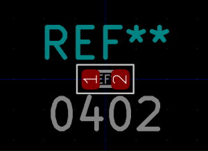
The 0.8 mm thick tracks do connect to a pair of such capacitors, but only after reducing the minimal clearance to 0.15 mm (which is the wrong thing to do):
It’s quite evident that the tracks are all over the pads. This isn’t all that bad, because the solder mask is still correct (not visible on image above). And yet, the tracks get too close to each other, and they’re not supposed to extend the pads on the copper layer.
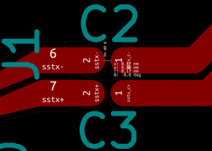
So this is what an extended 0402 looks like, with the beginning of a 0.8 mm track on each side:
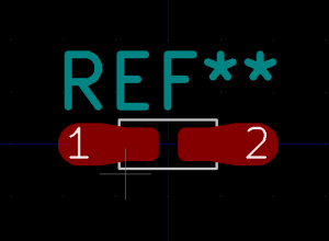
Each pad actually consists of three elements: The original pad (without the pad number), a filled polygon and a circular pad, which has the pad number assigned to it.
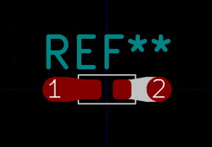
Moving these elements apart a bit for clarity, it looks like this:
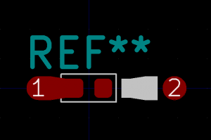
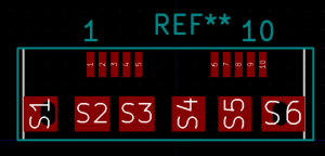
But the real need for this technique came from the USB 3.0 receptacle’s footprint, having pads too small for the 0.8 mm tracks:
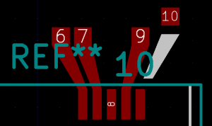
To overcome this, extension were added, making pads 0.8 mm wide and 0.2 mm apart. The pad is square in this example, so the track can only arrive directly from above:
Pad 10 of the image above has been separated for the sake of demonstration.
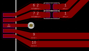
This is what the result looks like in a PCB design using these:
Exaggerated perfectionism or the right thing for a 5 or 10 GHz signal, who knows.
How to do this
A pad with type Custom (having rectangular or circular anchor) can be merged with any number of geometrical shapes, turning it into a larger pad, with the shape of the union of all merged areas.
So:
- Draw a filled polygon (on the F.Silk for example) and then change its line thickness to 0.
- Create a pad with “Shape” set to “Custom (Rect. Anchor)”, which will be the actual pad that the wire will be connected to.
- Select both, right-click, and pick “Create Pad from Selected Shapes”.
The attributes (which layers etc.) are taken from the anchor pad, but the shape is the union of the pad and the polygon. As mentioned above, a circular anchor pad with the diameter of the track width is easiest to work with later (but more difficult to match the polygon for).
In fact, getting the polygons just right is a bit of a headache. I found myself editing the polygons’ coordinates manually in the footprint files to get exact positions. The “Move Exactly” feature is also helpful for placing items accurately.
Note that the extra pad (actually, the anchor pad) should be designated for the copper layer only: No solder mask nor paste layers. We define it as a pad so a track will connect to it, but it’s not going to be soldered on.
What about the courtyard? Should it be extended? Well, no: There’s no problem having other components placed over the extended area, which is part of the wiring. PCBnew ensures no other copper traces get near by virtue of clearance requirements.
Having said all this, note that the trickery with “Create Pad from Selected Shapes” isn’t really necessary. It just makes it simpler to manipulate the shapes as one unit. It also moves the filled polygon from its original layer to the copper layer, but that can be done on the polygon’s own attributes. This way or another, the track connects to the anchor pad (in the merged version) or a simple pad. It doesn’t really matter if the extra geometry is linked to the pad or not.
But now we have two pads
There is the original pad, which is left in place, partly for laziness: It’s already at the right size and place, covering the correct layers (including solder mask and paste), so why mess with it? And then there’s the new pad, which is part of the extension, only for the copper layer.
The question is whether the original pad should also have the pin number, or if it should be pinless. There are basically three options:
- Keep the pin number, so both pads have the same number. In this case, PCBnew requires both pads to be connected (wires explicitly with tracks) or the original pad is considered unconnected, and will generate a DRC error. Signing off a PCB layout with unconnected nets errors requires a certain amount of courage. And drawing the internal wire without adding dirt may be tricky.
- Remove pin number designation from original pad. But this will cause PCBnew to complain that the new and original pads are too close (in fact, they’re touching). They are considered two different pads, and generate a DRC error like the following:
ErrType(19): Pad too close to pad
    @(201.775 mm, 57.300 mm): Pad of J1 on F.Cu and others
    @(204.850 mm, 57.950 mm): Pad 9 of J1 on F.Cu
Well, in some cases this can be solved by skipping the “Create Pad from Selected Shapes” part, and have two (non-custom) pads, with the filled polygon on the copper layer between them, and hence also making enough space between the pads. It’s a question of the size of the polygon vs. the required pad clearance.
- Replace the original pad with plain graphics, drawing it as three distinct and overlapping polygons: One for the copper layer, one for the solder mask and one for the solder paste. Rounded corner are achieved with the polygon’s line thickness, if so desired. Haven’t tried this (it’s a bit tedious, after all), but it should work. Note that just merging the original pad’s geometry into the new pad will only cover the copper layer (as the new pad is defined not to cover the two other layers).
I went for the second option, because I allow myself to ignore DRCs on pad-to-pad clearances, but not unconnected net errors. If pad-to-pad clearances are violated because of components placed too close, courtyards are there to prevent them. So making a habit of ignoring pad-to-pad DRC errors is fairly OK.
Impact on signal integrity
I started with this pad manipulation thing because I thought I had no choice, but then I asked myself what this does to the signals. Short answer: I don’t really know, because I haven’t run an electromagnetic simulation on this.
But the word is that any sudden change and discontinuity causes reflections, so connecting to a pad with a gradually changing track width should be better. Maybe, one day, there will be a KiCad feature making all or selected connections between pads and tracks adapting this way.
In fact, think of a thin wire connected to a thicker pad. Wouldn’t it be better if it became gradually thicker as it approaches the pad, so there’s no discontinuity there?
Or maybe it won’t make enough difference to care about this at all. Once again, I don’t know. I guess it’s something the RF guys care more about, and much less us dealing with digital signals.
I should also mention that the way that the pads go sideways on the receptacle shown above, creates a certain difference in the track length, which isn’t accounted for. One can measure the difference manually and feed it into “Pad to die length” in the pad’s attributes, but that was a bit too much for me.
