Oscilloscope views of the i.MX51′s EIM bus in action
These are a few oscilloscope samples, some of which are pretty crude, showing Freescale’s i.MX51 accessing its address/data bus.
I worked with an Armadeus APF51 board, which has a 16-bit multiplexed bus connected to the Xilinx Spartan-6 FPGA. The FPGA was used to wire bus signals to a pin header, so 1-2 ns skews between signals are possible.
I wrote some code for the FPGA and processor on the board, for the sake of making these samples, which is available in another post of mine. I also wrote a general post about the EIM bus, which may come handy.
A simple write cycle
With the default settings mentioned here, detailed registers in hex follow:
CS2GCR1=019100bf, CS2GCR2=00000000
CS2RCR1=01000000, CS2RCR2=00000008
CS2WCR1=01000000, CS2WCR2=00000000
WEIM Config register WCR=00000021
WEIM IP Access register WIAR=00000014
CCM_CBCDR=59ab7180
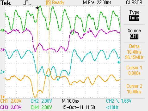
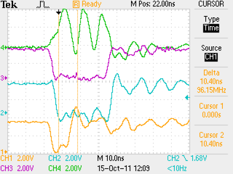
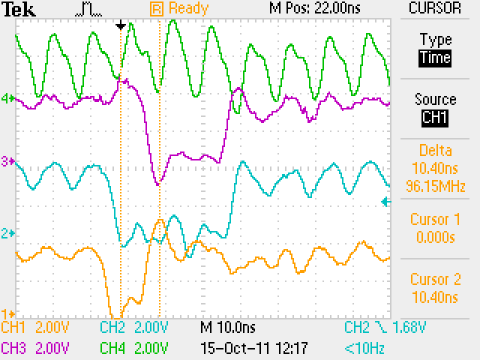
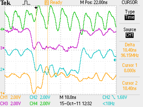
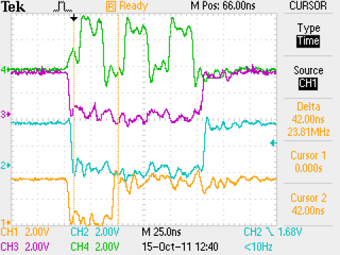
Traces from top to bottom (CH4 to CH1): BCLK, WE, CS2 and ADV (trigger on falling edge of CS2).
The BCLK doesn’t look much like a clock, and the signals are cluttered since the clock frequency is 95 MHz, the oscilloscope’s bandwidth is 200 MHz and the signals are picked up with simple probes from the FPGA pin header, so there’s a lot of crosstalk and other issues. But it’s good enough to see the general picture.
You’ll have to believe me that the address is present on the multiplexed address/data lines while the ADV is low (one clock cycle) and that the two other clock cycles carry the two data halves of the 32 bit word (the data width is only 16 bits). Honestly. I checked it out.
What can be seen barely in the scope image is that the bus signals switch on BLK’s falling edges, and that they should be sampled on BCLK’s rising edges. But hey, that exactly what the datasheet says in section 4.6.7.3, table 53.
With non-continuous clock
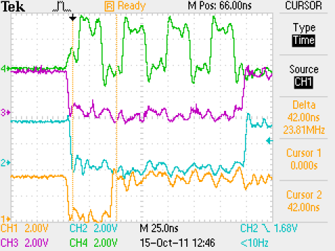
The same as above, now with BCM=0, so the BCLK toggles only when the bus is working:
CS2GCR1=019100bf, CS2GCR2=00000000
CS2RCR1=01000000, CS2RCR2=00000008
CS2WCR1=01000000, CS2WCR2=00000000
WEIM Config register WCR=00000020
WEIM IP Access register WIAR=00000014
Nothing really interesting about this, actually.
Delaying the assertion of WE
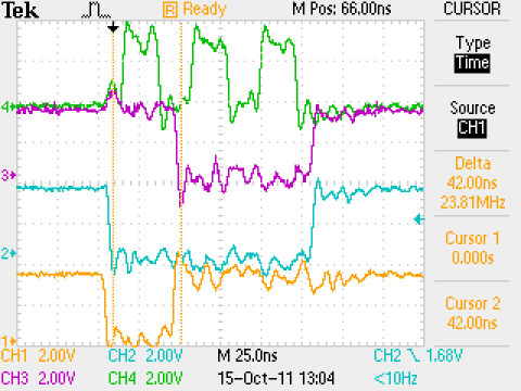
Returning to the continuous clock, let’s delay WE by one WEIM clock (which happens to be one BCLK) by setting WEA=1
CS2GCR1=019100bf, CS2GCR2=00000000
CS2RCR1=01000000, CS2RCR2=00000008
CS2WCR1=01000200, CS2WCR2=00000000
WEIM Config register WCR=00000021
WEIM IP Access register WIAR=00000014
And nothing really happened here, including the other signals, which are not shown. Except that WE was indeed asserted later.
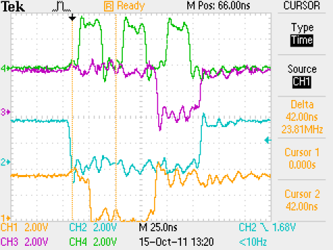
Adding a wait state
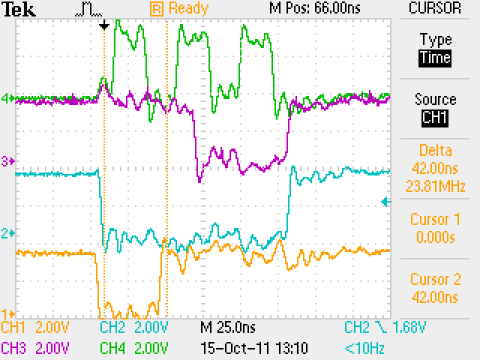
With the “simple write cycle” as the starting point, setting WWSC=2 (its default is 1) an extra wait state cycle is added:
CS2GCR1=019100bf, CS2GCR2=00000000
CS2RCR1=02000000, CS2RCR2=00000008
CS2WCR1=02000000, CS2WCR2=00000000
WEIM Config register WCR=00000021
WEIM IP Access register WIAR=00000014
Again, you’ll have to believe me that the first 16-bit data word is on the bus on both the second and third BCLK cycle. That is, the waitstate dwells on the first piece of data.
By the way, the waitstate count for read bursts was changed here as well, but that’s irrelevant. It’s just something my test kit did.
Bus clock division
To get a cleaner look, the next scope traces will be done with BCD=3, so the clock is divided by four. Continuous BCLK is also disabled by setting BCM=0, or otherwise there is no phase relation between BCLK and the bus signals.
So just by making these two changes relative to the “simple write cycle” we have
CS2GCR1=019130bf, CS2GCR2=00000000
CS2RCR1=01000000, CS2RCR2=00000008
CS2WCR1=01000000, CS2WCR2=00000000
WEIM Config register WCR=00000020
WEIM IP Access register WIAR=00000014
The time sweep is slower in this scope image, of course.
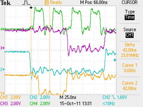
Bus clock division + adding a wait state
With the last trace as the starting point, setting WWSC=2 (its default is 1) an extra wait state cycle is added:
CS2GCR1=019130bf, CS2GCR2=00000000
CS2RCR1=02000000, CS2RCR2=00000008
CS2WCR1=02000000, CS2WCR2=00000000
WEIM Config register WCR=00000020
WEIM IP Access register WIAR=00000014
So we have four BCLKs instead of three, as one should expect.
A read cycle
Keeping the bus division (BCD=3 and BCM=0), and reverting everything else to the original setting, we’ll have a look on a read cycle. There’s no point in sampling WE anymore, so the probe moves to the OE signal instead. All in all, the traces from top to bottom (CH4 to CH1) are from now on: BCLK, OE, CS2 and ADV (trigger on falling edge of CS2).
CS2GCR1=019130bf, CS2GCR2=00000000
CS2RCR1=01000000, CS2RCR2=00000008
CS2WCR1=01000000, CS2WCR2=00000000
WEIM Config register WCR=00000020
WEIM IP Access register WIAR=00000014
As expected, there are two clock cycles with OE low. This is where the processor expects to get some data.
Delaying OE assertion
With the previous example as a starting point, setting OEA=2 yields the following:
CS2GCR1=019130bf, CS2GCR2=00000000
CS2RCR1=01002000, CS2RCR2=00000008
CS2WCR1=01000000, CS2WCR2=00000000
WEIM Config register WCR=00000020
WEIM IP Access register WIAR=00000014
This may come as a surprise: The OE’s assertion point was delayed by two WEIM clocks, which happens to be half a BCLK cycle. And nothing else changed.
Delaying ADV assertion
With “A read cycle” as a starting point, setting RADVA=2 yields the following:
CS2GCR1=019130bf, CS2GCR2=00000000
CS2RCR1=01200000, CS2RCR2=00000008
CS2WCR1=01400000, CS2WCR2=00000000
WEIM Config register WCR=00000020
WEIM IP Access register WIAR=0000001
What we can see here, is that the ADV signal was delayed, but not shortened. While OE’s deassertion point didn’t move, ADV’s did move as a result of delaying the assertion. What is not visible in this scope image, is that the processor keeps driving the address on the address/data lines as long as ADV is asserted, leaving less time for data (as evident by the shortened OE).
Delaying ADV assertion and deassertion
Setting RADVN=2 on top of the previous example, we have a two WEIM clock delay on both the assertion and deassertion, so the deassertion is delayed by 4 WEIM clocks, which is one BCLK. Or in simple words, the first data cycle is completely wiped out:
CS2GCR1=019130bf, CS2GCR2=00000000
CS2RCR1=01220000, CS2RCR2=00000008
CS2WCR1=01480000, CS2WCR2=00000000
WEIM Config register WCR=00000020
WEIM IP Access register WIAR=0000001
I don’t know if this setting is legal, but it was pretty evident that the data read by the processor during these cycles wasn’t consistent, not even the 16 LSB, which are read during the buried cycle.
Making it OK
Just to have a happy ending, let’s add a wait state. This will pull out the overridden data cycle and make the whole bus operation normal again.
So with RADVA=RADVN=2 and RWSC=2 (with the default as RWSC=1, this means a wait state) we have
CS2GCR1=019130bf, CS2GCR2=00000000
CS2RCR1=02220000, CS2RCR2=00000008
CS2WCR1=02480000, CS2WCR2=00000000
WEIM Config register WCR=00000020
WEIM IP Access register WIAR=0000001
So all in all there’s a longer ADV assertion, which is compensated with a wait state, so there’s time for both data cycles.

Reader Comments
Why not connect the GND signal in a better way ?
Maybe the 4 tracks you read better.
Kappasm
I tried a few ground sources. Unfortunately, this is as good as it gets.