Ultrascale GTH transceivers: Advanced doesn’t necessarily mean better
Introduction
I tend to naturally assume that newer FPGAs will perform better in basically everything, and that the heavier hammers are always better. Specifically, I expect the GTX / GTH / GT-whatever to perform better with the newer FPGAs (not just higher rates, but simply work better) and that their equalizers will be able to handle lousier input signals. And that the DFE equalizer will perform better than its little brother, LPM, in particular when the signal has been through some stuff.
And then there’s reality. This post summarizes my own findings with a USB 3.0 (SuperSpeed) link from the host to the FPGA, running at 5 Gb/s raw data rate on wire, with scrambler enabled. There is no official support for USB 3.0 by Xilinx’ transceivers, however the link parameters resemble those of SATA (in particular the SSC clocking without access to the clock), so I used the recommended settings for SATA, except for changing the data rate and reference clock frequency.
I’ll focus on Ultrascale’s GTH transceiver as well as the DFE equalizer, neither of which performed as I expected.
There’s a brief explanation on equalizers and related issues at bottom of this post, for those who need some introduction.
And ah, not directly related, but if a complete design example with an Ultrascale GTH would help, here’s one. Actually, there’s also the same for earlier FPGAs (7-series).
Choosing insertion loss on Ultrascale
The setting of Transceiver IP Wizard for Ultrascale and Ultrascale+ has a crucial difference regarding the receiver: Under the “Advanced” section, which is hidden by default, the physical characteristics of the channel can be set. Among others, the equalizer can be selected between “Auto” (default), “LPM” and “DFE”. This selection can be done with the Wizard for Kintex-7 and Virtex-7 FPGAs as well, but there’s a new setting in the Ultrascale Wizard: The insertion loss at the Nyquist frequency.
The default for Ultrascale, with SATA preset, is 14 dB insertion loss, with the equalizer set to Auto. The actual result is that the GTH is configured automatically by the Wizard to use the LPM equalizer. The insertion loss is quite pessimistic for a SATA link (and USB 3.0 as well), but that doesn’t matter so much, given that LPM was chosen. And it works fine.
But knowing that I’m going to have reflections on the signal, I changed the equalizer from “Auto” to “DFE”. I was under the wrong impression that the insertion loss was only a hint for the automatic selection between LPM and DFE, so I didn’t give it any further attention. The result was really poor channel performance. Lots of bit errors.
Investigating this, I found out that while the insertion loss setting doesn’t make any difference with the LPM equalizer (at least not in the range between 0 and 14 dB), it does influence the behavior of DFE. Namely, if the insertion loss is 10 dB and below, the DFE’s AGC component is disabled, and a fixed gain is assigned instead. More precisely, the GTHE3_CHANNEL primitive’s RXDFEAGCOVRDEN port is assigned a logic ’1′, and RXDFE_GC_CFG2 instantiation parameter is set to 16′b1010000 instead of all zeros.
So apparently, the DFE’s AGC doesn’t function properly unless the signal arrives with significant attenuation. This isn’t problematic when the physical link is fixed, and the insertion loss can be calculated from the PCB’s simulation. However when the link involves a user-supplied cable, such as the cases of USB 3.0 and SATA, this is an unknown figure.
Given that the insertion loss of cables is typically quite low, it makes sense to pick an insertion loss of 10 dB or less if DFE is selected. Or just go for LPM, which is configured exactly the same by the Wizard, regardless of the insertion loss setting (for the 0 dB to 14 dB range, at least). As the eye scans below show, the DFE wasn’t such a star anyhow.
In this context, it’s interesting that the Wizard for 7-series FPGAs (Kintex-7, Virtex-7 and Artix-7) doesn’t ask about insertion loss. You may select DFE or LPM, but there’s no need to be specific on that figure. So it seems like this is a workaround for a problem with the DFE on Ultrascale’s transceivers.
DFE vs. LPM on Ultrascale
As the eye scans shown below reveal, it turns out that DFE isn’t necessarily better than LPM on an Ultrascale FPGA. This is somewhat surprising, since LPM consists of a frequency response correction filter only, while the transceiver’s DFE option includes that on top of the DFE equalizer (according to the user guide). One could therefore expect that DFE would have a better result, in particular with a link that clearly produces reflections.
This, along with the Wizard’s mechanism for turning off the AGC for stronger signals, seems to indicate that the DFE didn’t turn out all that well on Ultrascale devices, and that it’s better avoided. Given that it gave no benefit with a 5 Gb/s signal that goes through quite a few discontinuities, it’s questionable whether there is a scenario for which it’s actually the preferred choice.
Eye scans: General
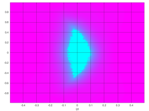
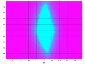
I’ve made a lot of statistical eyes scans for the said USB channel. This mechanism is made by Xilinx’ transceivers themselves, and is described in the respective user guides. In a nutshell, these scans show how the bit error rate is affected by moving the sampling time from the point that the CDR locks on, as well as adding a voltage offset to the detection threshold. The cyan-colored spot in the middle of the plots shows the region of zero bit errors, and hence it size displays the margins in time and voltage for retaining zero BER.
The important part is the margin in time. In the plots below, UI is the time unit used. One UI corresponds to a bit’s period (i.e. the following bit appears at UI = 1). The vertical axis is less well defined and less important, since voltage is meaningless: It can be amplified as needed. The shape of the eye plot can however give a hint sometimes about certain problems.
The plots in this post were all made on a USB 3.0 data stream (running at the standard 5 Gb/s with scrambler applied), created by a Renesas uPD720202 USB controller (PCI ID 1912:0015), received by the FPGA’s transceiver.
The physical connection, except for PCB traces, involved a Type A connector, connected to a Micro B connector with a high-quality 1 meter USB cable. The Micro-B connector is part of an sfp2usb adapter, which physically connects the signal to the SFP+ connector inside an SFP+ cage, which in turn is connected directly to the FPGA. The signal traces of the sfp2usb adapter are about the length of the SFP+ cage.
So overall, it’s the USB controller chip, PCB trace, USB type A connector mating, 1 meter of cable, Micro B connector mating, a short PCB trace on the sfp2usb adapter, an SFP+ connector mating, PCB trace on the FPGA board reaching the FPGA’s transceiver.
The Renesas USB controller was selected over other options because it showed relatively low signal quality compared with other USB signal sources. The differences are more apparent with this source, however the other sources all gave similar results.
Needless to say, testing at a specific rate with specific equipment doesn’t prove anything on the general quality of the transceivers, and yet the 5 Gb/s represents a medium rate channel quite well.
The FPGA boards used:
- Xilinx KCU105 for Kintex Ultrascale
- Xilinx KC705 for Kintex-7
- Trenz TE0714 for Artix-7 with carrier board having an SFP+ cage
I used some home-cooked logic for making the eye scans and Octave to produce the plots, so if the format doesn’t look familiar, that’s why.
LPM vs. DFE with Ultrascale GTH
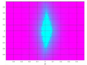
This is the eye scan plot for LPM (click to enlarge the plots):
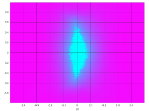
And this is for DFE, with insertion loss set below the 10 dB threshold:
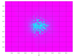
And this is DFE again, with insertion loss set to 14 dB:
It’s quite evident that something went horribly wrong when the insertion loss was set to 14 dB, and hence the AGC was enabled, as explained above. But what is even more surprising is that even with the AGC issue away, the eye scan for DFE is slightly worse than LPM. There are three connectors on the signal paths, each making its reflections. DFE should have done better.
Comparing DFE scans with Kintex-7′s GTX
Here’s the proper DFE eye scan for Ultrascale’s GTH again (click to enlarge):
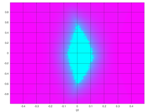
And this is Kintex-7, same channel but with a GTX, having considerably less equalizer taps:
It’s quite clear that the zero-BER region is considerably larger on the Kintex-7 eye scan. Never mind the y-axis of the plot, it’s the time axis that matters, and it’s clearly wider. Kintex-7 did better than Ultrascale.
Comparing LPM scans with GTX / GTP
This is the LPM eye scan for Ultrascale’s GTH again:
And Kintex-7′s counterpart:
It’s clearly better than Ultrascale’s scan. Once again, never mind that the zero-BER part looks bigger: Compare the margin in the time axis. Also note that Kintex-7′s DFE did slightly better than LPM, as expected.
And since Artix-7 is also capable of LPM, here’s its scan:
Surprise, surprise: Atrix-7′s eye scan was best of all options. The low-cost, low-power device took first prize. And it did so with an extra connector with the carrier board.
Maybe this was pure luck. Maybe it’s because the scan was obtained with a much smaller board, with possibly less PCB trace congestion. And maybe the LPM on Artix-7 is better because there’s no DFE on this device, so they put an extra effort on LPM.
Conclusion
The main takeaway from this experience of mine is that advanced doesn’t necessarily mean better. Judging by the results, it seems to be the other way around: Ultrascale’s GTH being more fussy about the signal, and losing to Kintex-7′s GTX, and both losing to Artix-7.
And also, to take the insertion loss setting in the Wizard seriously.
As I’ve already said above, this is just a specific case with specific equipment. And yet, the results turned out anything but intuitive.
Appendix: Equalizers, ISI and Nyquist frequency, really briefly
First, the Nyquist frequency: It’s just half the raw bit rate on wire. For example, it’s. 2.5 GHz for a USB Superspeed link with 5 Gb/s raw data rate. The idea behind this term is that the receiver makes one analog sample per bit period, and Nyquist’s Theorem does the rest. But it’s also typically the frequency at which one can low-pass filter the channel without any significant effect.
Next, what’s this insertion loss? For those who haven’t played with RF network analyzers for fun, insertion loss is, for a given frequency, the ratio between the inserted signal power on one side of the cable and/or PCB trace and the power that arrives at the other end. You could call it the frequency-dependent attenuation of the signal. As the frequency rises, this ratio tends to rise (more loss of energy) as this energy turns into radio transmission and heat. Had this power loss been uniform across frequency, it would have been just a plain attenuation, which is simple to correct with an amplifier. The frequency-varying insertion loss results in a distortion of the signal, typically making the originally sharp transitions in time between ’0′ and ’1′ rounder and smeared along possibly several symbol periods.
This smearing effect results in Intersymbol Interference (ISI), which means that when the bit detector samples the analog voltage for determining whether its a ’0′ or ’1′, this analog voltage is composed of a sum of voltages, depending on several bits. These additional voltage components act a bit like noise and increase the bit error rate (BER), however this isn’t really noise (such as the one picked up by crosstalk or created by the electronics), but rather the effect of a bit’s analog signal being spread out over a longer time period.
Another, unrelated reason for ISI is reflections: As the analog signal travels as an electromagnetic wave through the PCB copper trace or cable, reflections are created when the medium changes or makes sharp turns. This could be a via on the PCB board (or just a poorly designed place on the layout), or a connector, which involves several medium transitions: From the copper trace on the PCB to the connector’s leg, from one side of the connector to the connector mating with it, and then from the connector’s leg to the medium that carries the signal further. This assuming the connector doesn’t have any internal irregularities.
So ISI is what equalizers attempt to fix. There’s a relatively simple approach, employed by the linear equalizer. It merely attempts to insert a filter with a frequency response that compensates for the channel’s insertion loss pattern: The equalizer amplifies high frequencies and attenuates low frequencies. By doing so, some of the insertion loss’ effect is canceled out. This reverse filter is tuned by the equalizer for optimal results, and when this works well, the result is an improvement of the ISI. The linear equalizer doesn’t help at all regarding reflections however.
The transmitter can help with this matter by shaping its signal to contain more high-frequency components — this is called pre-emphasis — but that’s a different story.
The DFE (Decision Feedback Equalizer) attempts to fix the ISI directly. It’s designed with the assumption that the transmitted bits in the channel are completely random (which is often ensured by applying a scrambler to the bit stream). Hence the voltages that are sampled by the bit detector should be linearly uncorrelated, and when there is such correlation, it’s attributed to ISI.
This equalizer cancels the correlation between the bit that is currently detected and the analog voltages of a limited number of bits that will be detected after it. This is done by adding or subtracting a certain voltage for each of the signal samples that are used for detecting the bits after the current one. The magnitude of this operation (which can be negative, of course) depends on the time distance between the current bit and the one manipulated. Whether its an addition or subtraction depends on whether the current bit was detected as a ’0′ or ’1′.
The result is hence that when the sample arrives at the bit detector, it’s linearly uncorrelated with the bits that were detected before it. Or more precisely, uncorrelated with a number of bits detected before it, depending on the number of taps that the DFE has.
This method is more power consuming and has a strong adverse effect if the bits aren’t random. It’s however considered better, in particular for canceling the effect of signal reflections, which is a common problem as the analog signal travels on the PCB and/or cable and reaches discontinuities (vias, connectors etc.).
Having said that, one should remember that the analog signal typically travels at about half the speed of light on PCB traces (i.e. 1.5 x 10^8 m/s), so e.g. at 5 Gb/s each symbol period corresponds to 3 cm. Accordingly, an equalizer with e.g. 8 taps is able to cancel reflections that have traveled 24 cm (typically 12 cm in each direction). So DFE may help with reflections on PCBs, but not if the reflection has gone back and forth through a longer cable. Which may not an issue, since the cable itself typically attenuates the reflection’s signal as it goes back and forth.
According to the user guides, when a Xilinx transceiver is set to LPM (Low Power Mode), only a linear equalizer is employed. When DFE is selected, a linear equalizer, followed by a DFE equalizer are employed.

Reader Comments
I’ve been spending significant amount of time dealing with Xilinx Ultrascale transceivers, and squeezing every bit of performance out of them. Specifically, for supporting latest USB 4, PCIe Gen5, and 200/400 GbE specs. Whatever settings transceiver IP wizard provides are not going to achieve the best possible performance, that’s for sure. You’d need to work with your FAE to get a few settings for RXDFE_GC_CFG2 and other undocumented registers that might work better for your specific channel and SSC clock. I even found experimentally that completely turning off automatic DFE adaptation and running custom algorithm (reading DFE and gain stats from Digital Monitor interface) did improve performance.
We’re just now also in the situation, where the LPM equalizer shows better performance than the DFE on Ultrascale’s GTH.
Eli, or maybe Evgeni, do you perhaps have any idea if we could override 10 out of the 11 DFE taps to 0? The idea is to try DisplayPort’s reference DFE, which has just one tap.
Of course, Xilinx offers no support in modifying the DFE in their official documentation.