Hierarchies in Orcad schematics: Please, don’t
It seems like hierarchies are to board designers what C++ is to programmers: It kills the boredom, but also the project. They will proudly show you their block diagrams and the oh-so-ordered structure, but in the end of the day, noone can really figure out what’s connected to what. Which is kinda important in a PCB design.
Not to mention that it’s impossible to tell what’s going on looking at the pdf schematics: Try to search for the net’s name, and you’ll find it in 20 places, 18 of which are the inter-hierarchy connections of that net. One of which, is maybe wrong, but is virtually impossible to spot.
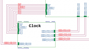
On a good day, everything looks fine and in order, and noone notices small killers like the one below. It’s easy (?) to spot it now that I’ve put the focus on it, but would you really see this on page 23 of yet another block connection in the schematics?
Click to enlarge (this is from a real-life design made by a serious company):
 So please, PCB designers, wherever you are: Look at any reference design you can find, and do the same: Just put the net names that belong to another page. Don’t try to show the connections between the blocks. They help nobody. If the net name is meaningful, we will all understand on which page to look for it. And if we don’t, we use our pdf browser’s search feature. Really.
Reader Comments
So true! And if you think it’s bad in Orcad, pray you never get forced to use (x)DxDesigner!
Mmm, we are going the other way.
Dx to Orcad, which does not look good to me.
The only way to create hierarchy is top-down. If you have the right tools, they will add hierarchy ports with the correct name as you add the connections. Push down and the job’s a good’un.
Good point about navigating PDFs. I hate them.
It would help a lot if the PDF printer added the page number to each hierarchy block, but then that would be far too hard to automate, eh?
Orcad way of naming net is pretty straightforward in herarchical designs.
Net name can come from upper level.
If there is a conflict, net is renamed NAME_INSTANCENAME
You can find PCB nets in schematics by searching by flat nets.
Sometimes in my schematics, the same page is used 16 times. In this case having a hierarchical schematic is a must.
It helps also to have consistency accros schematics and it facilitate schematic page reuse.
I would not live without hierarchical design :)