Introduction
This page discusses source-synchronous data inputs: This technique means that the data inputs are synchronous with a clock that the external component generates in parallel with these inputs.
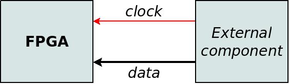
This method is often used simply because this is the way the external component works. Another good reason is that the source of the data is physically far away from the FPGA. It's also possible that there is a cable and connector between the FPGA and the other side. For example, a digital camera that sends pixel data.
A possible difficulty with a source-synchronous clock is that it may not be active all the time. The clock signal may also be affected by a dangling physical connection or excessive noise. It's also possible that the clock doesn't have a steady clock period, or that the jitter is excessively high. This happens often when the source of the data (and hence also the clock) is a microprocessor's I/O peripheral.
Note that there is a separate page that discusses the relations between clock and data in general.
Coping with an unstable clock
The most important guideline with source-synchronous inputs is that the clock should not be connected directly to logic elements inside the FPGA. Rather, the clock that is used inside the FPGA should be a clean clock, which is generated by a PLL that is inside the FPGA.
If an external clock is connected directly to logic inside the FPGA, there may be weird problems: A bad clock creates unexpected behaviors that don't look like a problem with a clock. Excessive jitter and glitches may violate the timing requirements that ensure the design's reliable operation. The consequence is that virtually anything can happen, including situations that are impossible according to the Verilog code. It's therefore easy to mistakenly think that the problem is a bug in the FPGA design.
It's natural to (mistakenly) think that problems with a clock only cause a loss of clock cycles, and consequently some data elements will be missing. When a bad clock causes other problems, the attempts to solve this problem are often focused on the parts of the logic design that seem most related. That can waste a lot of time.
The only situation where an external clock can be used directly by the logic fabric is when this clock is guaranteed to be stable and clean. If this clock isn't stable when the FPGA begins to operate, this issue requires treatment: As long as the clock is unstable, a reset must be applied to the logic that relies on this clock.
Possible strategies
There are mainly four possible strategies for synchronizing with the external clock. These strategies are discussed below, in no particular order.
Strategy #1: 01-signal sampling
This strategy is the most robust method for source-synchronous inputs. When the external clock is misbehaving, 01-signal sampling has a clear advantage over any other method. However, this method is useful only when the frequency of the data source's clock is relatively low.
This method is discussed separately on a dedicated page.
Strategy #2: Using a PLL
With this strategy, the external clock is connected to the input of a PLL on the FPGA. This PLL's output clock is used for the logic elements. A reset signal is applied to these logic elements when the PLL is not locked. This solution ensures that the logic elements rely on a stable clock: When the PLL's output clock isn't stable, the logic elements are deactivated by the reset.
The PLL also makes it easier to achieve the timing requirements, compared with connecting the external clock directly: The PLL compensates for the delay between the clock pin and the FPGA's internal clock.
However, note that imperfections of the external clock can cause excessive jitter at the PLL's output. The PLL's lock detector may continue to indicate that the PLL operates properly, even though the clock that it produces is unusually noisy. There is no simple solution to this situation. One possibility is to change the timing constraints for the logic that depends on the PLL's output. For example, the clock's jitter in the timing constraints can be increased to a value that the PLL will probably not exceed (because a loss of lock would occur).
There is a similarity between this strategy and system synchronous clocking: In both scenarios, the external clock is connected to a PLL, and the output of this PLL is used inside the FPGA. The timing constraints are hence written in the same way as for a system synchronous clock.
Note that the PLL usually aligns its output clock with the external clock in a way that is optimal for a system synchronous clock. The optimal alignment for a source synchronous clock may be slightly different. In both possibilities, the clocks aren't perfectly aligned. Rather, there's an intentional small time difference between the clocks' edges. This time difference makes it easier to meet the timing requirements of the I/O registers. Some PLLs can be configured to align the clocks for optimal performance with a source synchronous clock.
This strategy is the easiest one to implement, compared with the other strategies that are listed here. It's suitable for relatively high clock frequencies. But for frequencies that are close to the maximum of what the I/O is capable of, this strategy will probably not work.
Strategy #3: Phase shifting
This strategy is usually chosen when the data rate is close to the maximum that the FPGA can support.
The usual ways for guaranteeing the timing requirements will not work at such data rates: It will be impossible to achieve the timing constraints. However, a reliable sampling of the data signals is still possible.
The problem with timing constraints is to ensure the timing requirements through a calculation: Such calculation includes several uncertain parameters, e.g. differences in the manufacturing of the FPGA. When these parameters are taken into account, calculations will not yield a timing solution that ensures a reliable sampling. When the data rate is very high, there is no timing surplus to waste on these uncertainties.
But for a specific FPGA chip, these parameters are constant. The solution is hence to search for the correct timing while the FPGA is working. In practice, this means that a state machine inside the FPGA adjusts the delay between the the data clock and the moment of sampling. So an adaptive mechanism is used to find the optimal timing, rather than relying on calculations. This mechanism is called phase shifting.
This strategy is often used with the data signals from DDR SDRAM memories. In this application, the goal is always to reach a data rate as high as possible. Hence the I/O ports' capabilities are pushed to their limit. As a result, phase shifting is the only way to ensure that the data inputs are sampled reliably: After the DDR memory has been initialized, a special sequence of data is written to the memory (the data signals to the memory are source-synchronous outputs, so there is no difficulty with the timing). The FPGA then repeatedly reads from the same part in the DDR memory. A state machine finds the optimal timing by gradually altering the delay of the sampling. The expected input data is known, because it's the same sequence of data that was previously written. The state machine can therefore easily evaluate how reliable the data is, and find the optimal delay.
An interesting feature of this mechanism is that the data clock can be ignored: The DDR memory is synchronized with the clock that the FPGA generates. This clock is the part of the source-synchronous outputs that are received by the DDR memory. It's therefore guaranteed that the data clock of the source-synchronous inputs has exactly the same frequency as the clock that is generated by the FPGA. The phase shifting mechanism can therefore rely on the internal clock instead of the clock that arrives along with the data. It doesn't matter that there's an unknown delay between these two clocks: The state machine finds the optimal timing regardless of this delay.
In fact, this is how this mechanism is usually implemented for DDR memories: Even though DDR memories have an source-synchronous clock (called a data strobe), the usual implementation of the phase shifting mechanism ignores this signal. The rationale is that it's more important to ensure that the data signals arrive reliably than to be aligned with the strobe.
So using phase shifting can eliminate the need for a data clock. An internal clock can be relied upon instead, if its frequency is guaranteed to be exactly the same as the data rate.
With this strategy, the purpose of the timing constraints is are the same as with regular IOB registers.
Strategy #4: Using the clock directly
This strategy is apparently the most straightforward one: The external clock is connected directly to flip-flops inside the FPGA. Something like this:
module top (
   input data_clk,
   input [7:0] data
);

   reg [7:0] data_samp;

   always @(posedge data_clk)
     begin
       data_samp <= data;

      [ ... ]
     end
As mentioned above, this strategy is usually not a good idea. The primary reason is that if @data_clk has a glitch, all logic that depends on this clock becomes unpredictable.
It can be reasonable to use an external clock this way if it's guaranteed to be clean and stable. But even if this is guaranteed, it may be difficult to achieve the timing requirements because of the delay between the clock pin and the flip-flops. Some FPGAs have special clock resources for the purpose of reducing this delay. This may require using a dedicated clock input pin and restrict the I/O ports to specific regions on the FPGA.
When the clock is used directly, the timing constraints are written in the same way as for a system synchronous clock.
The straightforward alternative for this strategy is to use a PLL, as suggested above. If the data clock isn't stable, 01-signal sampling should be considered.
Summary
It's not a coincidence that 01-signal sampling was mentioned first on this page, and that this strategy is described on a separate page: This is the method that is most recommended if the data rate is not higher than this method is capable of.
If other strategies are considered, it's important to pay attention to the data clock's stability. If a clock deviates from its allowed behavior (i.e. the clock period and maximal jitter), this can result is a permanent and irrecoverable malfunction of the related logic. Only a reset will bring back the logic to normal operation.
Using a PLL for generating a reliable clock improves the situation considerably: The PLL's output is reliable as long as its lock detector indicates so. A reset should be applied to this logic otherwise.